
Owner manual


MAXQ1004
1-Wire and SPI Authentication Microcontroller
4
Stresses beyond those listed under “Absolute Maximum Ratings” may cause permanent damage to the device. These are stress ratings only, and functional
operation of the device at these or any other conditions beyond those indicated in the operational sections of the specifications is not implied. Exposure to absolute
maximum rating conditions for extended periods may affect device reliability.
Voltage Range on All Pins (including V
DD
),
except DQ to GND ............................................-0.5V to +3.6V
Voltage Range on DQ Relative to GND ...............-0.5V to +6.0V
Continuous Output Current
Any Single I/O Pin ...........................................................35mA
All I/O Pins Combined .....................................................35mA
Continuous Power Dissipation (T
A
= +70NC)
Single-Layer Board (derate 16.9mW/NC above +70NC) ..1349.1mW
Multilayer Board (derate 25mW/NC above +70NC) ....2000mW
Operating Temperature Range .......................... -40NC to +85NC
Storage Temperature Range ............................ -65NC to +150NC
Lead Temperature (soldering, 10s) ................................+300NC
Soldering Temperature (reflow) ......................................+260NC
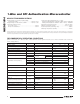
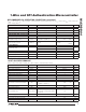
RECOMMENDED DC OPERATING CONDITIONS
(V
DD
= 1.7V to 3.6V, T
A
= -40NC to +85NC, unless otherwise noted. Typical values are at T
A
= +25NC and V
DD
= 3.3V, unless oth-
erwise noted.) (Note 1)
ABSOLUTE MAXIMUM RATINGS
PARAMETER SYMBOL CONDITIONS MIN TYP MAX UNITS
Supply Voltage V
DD
V
RST
3.3 3.6 V
1.8V Internal Regulator V
REG18
1.62 1.8 1.98 V
Power-On Reset Voltage V
POR
1.0 1.42 V
Power-Fail Reset Voltage V
RST
(Note 2) 1.64 1.695 V
Power-Fail Warning Voltage V
PFW
(Notes 3, 4) 1.75 1.85 V
Digital Overvoltage Detect V
HV
Monitors V
REG18
2.4 2.8 V
Supply Current (Note 5)
I
DD1
Device is executing
from flash
f
SYS
= 6MHz 3.5
mA
I
DD2
f
SYS
= 1MHz 0.8
Stop-Mode Current (Note 5)
I
STOP1
T
A
= +25NC, CPU not backed up
5
FA
I
STOP2
T
A
= +85NC, CPU not backed up
7.5
I
STOP3
T
A
= +25NC, CPU backed up
6.5
I
STOP4
T
A
= +85NC, CPU backed up
9
DIGITAL I/O
Input High Voltage (P0, RST)
V
IH
0.7 x
V
DD
V
DD
V
Input Hysteresis V
IHYS
(Note 6) 0.3 V
Input Low Voltage (P0, RST)
V
IL
V
GND
0.3 x
V
DD
V
Output Low Voltage (P0, RST)
(Note 7)
V
OL
V
DD
= 3.6V, I
OL
= 4mA (Note 6) 0.4
V
V
DD
= 1.85V, I
OL
= 4mA 0.4
Output High Voltage (P0, RST)
V
OH
I
OH
= -2mA
V
DD
-
0.4
V
DD
V
Input Leakage Current I
L
Internal pullup disabled -100 +100 nA
Input/Output Pin Capacitance C
IO
(Note 6) 15 pF
Input Low Current for All Pins I
IL
V
IN
= 0.4V, pullup enabled -70
FA
RST Pullup Resistor
R
RST
65
Q20% kI