
Owner manual


MAXQ1004
1-Wire and SPI Authentication Microcontroller
9
Pin Description (continued)
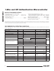
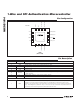
Block Diagram
MAXQ1004
16KB FLASH MEMORY
640B DATA SRAM
4KB UTILITY ROM
WATCHDOG TIMER
GND +1.7V TO +3.6V
INTERNAL
6MHz
OSCILLATOR
RANDOM-NUMBER
GENERATOR
AES ENCRYPTION
ENGINE
TEMP
SENSOR
INTERNAL
REFERENCE
10-BIT ADC
VOLTAGE
MONITOR
MAXQ RISC
CPU
GPIO
(UP TO 8)
SPI
JTAG
1-Wire
INTERFACE
TIMER 0
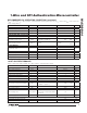
PIN NAME FUNCTION
GENERAL-PURPOSE I/O PINS
3–10
P0.0–P0.7,
INT0–INT7,
MOSI, MISO,
SCLK, SSEL,
TCK, TDI,
TMS, TDO
General-Purpose, Digital I/O, Type D Port/SPI Interface/JTAG Interface/External Edge-
Selectable Interrupt. This port functions as 8-bit I/O and as an alternate interface to external
interrupts. Each interrupt can be individually enabled and the active edge can be selected.
The default reset condition of the pins is as a weak pullup input. To drive port 0 as output, the
port direction register must be programmed to enable output. P0.7–P0.4 default to their JTAG
function on any reset.
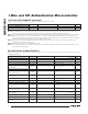
PIN PORT
EXTERNAL
INTERRUPT
SPECIAL FUNCTION
3 P0.0 INT0 MOSI: Master Out-Slave In (SPI)
4 P0.1 INT1 MISO: Master In-Slave Out (SPI)
5 P0.2 INT2 SCLK: Slave Clock (SPI)
6 P0.3 INT3
SSEL: Active-Low Slave Select (SPI)
7 P0.4 INT4 TCK: Test Clock (JTAG)/T0
8 P0.5 INT5 TDI: Test Data In (JTAG)/T0G
9 P0.6 INT6 TMS: Test Mode Select (JTAG)
10 P0.7 INT7 TDO: Test Data Out (JTAG)
2 DQ
1-Wire Slave Interface, I/O. This 5V tolerant, open-drain I/O pin serves as both transmit and
receive pin for the 1-Wire interface. The DQ pin requires an external pullup resistor, the value
of which is determined by the speed mode.