Rev 0; 1/09 Low-Power, Dual-Core Microcontroller The MAXQ3108 is a low-power microcontroller that features two high-performance MAXQ20 cores: a dedicated core (DSPCore) for intensive data processing and a user core (UserCore) for supervisory functions. The two cores can operate at different clock speeds, allowing lower system power consumption for even processing intensive applications.
MAXQ3108 Low-Power, Dual-Core Microcontroller TABLE OF CONTENTS Absolute Maximum Ratings . . . . . . . . . . . . . . . . . . . . . . . . . . . . . . . . . . . . . . . . . . . . . . . . . . . . . . . . . . . . . . . . . . . . . .4 Recommended DC Operating Conditions . . . . . . . . . . . . . . . . . . . . . . . . . . . . . . . . . . . . . . . . . . . . . . . . . . . . . . . . . . .4 Block Diagram . . . . . . . . . . . . . . . . . . . . . . . . . . . . . . . . . . . . . . . . . . . . . . . . . . . . . . . .
Low-Power, Dual-Core Microcontroller Dual-Core Interfaces . . . . . . . . . . . . . . . . . . . . . . . . . . . . . . . . . . . . . . . . . . . . . . . . . . . . . . . . . . . . . . . . . . . . . . . .59 DSP Code Memory . . . . . . . . . . . . . . . . . . . . . . . . . . . . . . . . . . . . . . . . . . . . . . . . . . . . . . . . . . . . . . . . . . . . . .60 Intercore Communications . . . . . . . . . . . . . . . . . . . . . . . . . . . . . . . . . . . . . . . . . . . . . . . . . . . . . . . . . . . . . . .
MAXQ3108 Low-Power, Dual-Core Microcontroller ABSOLUTE MAXIMUM RATINGS Storage Temperature Range .............................-65°C to +150°C Soldering Temperature...........................Refer to the IPC/JEDEC J-STD-020 Specification. Voltage Range on Any Pin except VDD with Respect to VSS ...........................-0.3V to VDD Voltage Range on VDD with Respect to VSS .........-0.3V to +3.6V Operating Temperature Range ...........................
Low-Power, Dual-Core Microcontroller (VDD = VRST to 3.6V, TA = -40°C to +85°C.) (Notes 1, 2) PARAMETER Input/Output Pin Capacitance SYMBOL CIO CONDITIONS Input Low Current All Pins IIL VIN = 0.4V Input-Leakage Current IL Internal pullup disabled Input Pullup Resistor (All Inputs) MIN TYP Guaranteed by design -100 RPU MAX UNITS 15 pF -30 μA +100 nA 60 k CLOCK SOURCE FLL Output Frequency fFLL CX1 = 32.768kHz FLL Output Accuracy fFLL CX1 = 32.768kHz 9.5 10.0 10.5 MHz 1.
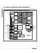
Low-Power, Dual-Core Microcontroller MAXQ3108 Block Diagram I0 P2.4/MDIN0P MANCHESTER DECODER CLK V0 I1 MANCHESTER DECODER CLK V1 I2 MANCHESTER DECODER CLK V2 SINC3 FILTER 24-BIT RESULT PULSE GENERATOR P2.5/CF1 SINC3 FILTER 24-BIT RESULT PULSE GENERATOR P2.6/CF2 SINC3 FILTER 24-BIT RESULT SINC3 FILTER 24-BIT RESULT SINC3 FILTER 24-BIT RESULT SINC3 FILTER MAXQ20 DSPCORE 4kW SRAM (CODE) 512W SRAM (DATA) MULTIPLYACCUMULATE UNIT 24-BIT RESULT MAILBOX COMM P2.3/MDIN0N/SSEL P2.
Low-Power, Dual-Core Microcontroller PIN NAME FUNCTION POWER PINS 21 VDD Supply Voltage. Must be bypassed with a 4.7μF capacitor with ESR < 5 and a 0.1μF ceramic capacitor. 17 GND Ground 20 REGOUT 19 VBAT Regulator Output. 1.8V output. Must be connected to a 1μF low-ESR (< 1 ) external ceramic chip capacitor. Battery Input for Backing Up the RTC CLOCK PINS 15, 16 CX1, CX2 RTC Crystal Inputs. The RTC requires a 32.768kHz crystal to be connected in order to supply the time base for the RTC.
MAXQ3108 Low-Power, Dual-Core Microcontroller Pin Description (continued) PIN NAME FUNCTION Port 2. Port 2 functions as both a 7-bit I/O port and as a special function interface to the CF pulse generator outputs, clock output, and the Manchester ENDEC or SPI. The default reset condition of the pins is weakly pulled up (input), with exception of P2.5 and P2.6, which are always outputs and default to strong high.
Low-Power, Dual-Core Microcontroller The MAXQ instruction set is designed to be highly orthogonal. All arithmetical and logical operations can use any register along with the accumulator. Data movement is supported from any register to any other register. Memory is accessed through specific data pointer registers with auto increment/decrement support. Memory The MAXQ3108 supports a pseudo-Von Neumann memory structure that can merge program and data into a linear memory map.
MAXQ3108 Low-Power, Dual-Core Microcontroller DSP Program RAM • In the SC register, bits CDA1 and UPM are not implemented since the size of the memory in the device does not require their implementation. A 4K Word (8KB) section of memory is available to the DSPCore as code memory. When the DSPCore is disabled (as it is immediately following a reset event) that block of memory appears in the UserCore data memory map at location 0x1000.
Low-Power, Dual-Core Microcontroller BIT REGISTER MOD: REG AD1LSB 0:9 ADC1 Output Register LSB AD2LSB 0:10 ADC2 Output Register LSB AD3LSB 0:11 ADC3 Output Register LSB AD4LSB 0:12 ADC4 Output Register LSB AD5LSB 0:13 MREQ0 0:14 MREQ1 0:15 15 14 13 12 11 10 9 8 7 6 5 4 3 2 1 0 ADC5 Output Register LSB REQCDV RSPIE ABF5 ABF4 REQCM Master Request Register 1 MREQ2 0:16 ADCN 0:17 Master Request Register 2 ADCC 0:18 MSTC 0:19 CCSL PO0 1:0 Port 0 Output Regis
MAXQ3108 Low-Power, Dual-Core Microcontroller Table 1.
Low-Power, Dual-Core Microcontroller BIT REGISTER MOD: REG AD0 0:0 0xFFFF AD1 0:1 0xFFFF AD2 0:2 0xFFFF AD3 0:3 0xFFFF AD4 0:4 0xFFFF AD5 0:5 0xFFFF SRSP0 0:6 SRSP1 0:7 AD0LSB 0:8 0xFF AD1LSB 0:9 0xFF AD2LSB 0:10 0xFF AD3LSB 0:11 0xFF AD4LSB 0:12 0xFF AD5LSB 0:13 MREQ0 0:14 MREQ1 0:15 MREQ2 0:16 ADCN 0:17 ADCC 0:18 MSTC 0:19 PO0 1:0 PO1 1:1 PI0 1:2 15 14 13 12 11 10 9 8 7 6 5 4 0 0 3 0 0 0 0 0 0 0 0 0 0 0x0 0 0x3 0x00 E
MAXQ3108 Low-Power, Dual-Core Microcontroller Table 2.
Low-Power, Dual-Core Microcontroller REGISTER MOD: REG TB0V 4:11 I2CCN 4:12 I2CCK 4:13 I2CTO 4:14 I2CSLA 4:15 BIT 15 14 13 12 11 10 9 8 7 6 5 4 0 0 0 3 2 1 0 0 0 0 0x0000 0 0 0 0 0x02 0x04 0x00 0x000 Peripheral Registers—DSPCore describes the functions associated with the peripheral registers, and Table 4 shows the default values of these registers. The MAXQ3108 DSPCore exposes its peripheral complement in modules numbered 0 and 1. Table 3 Table 3.
MAXQ3108 Low-Power, Dual-Core Microcontroller Table 3. DSPCore Peripheral Registers (continued) BIT REGISTER MOD: REG PO2 1:7 Port 2 Output Register MC1R 1:8 Multiplier Read Register 1 (MSB, bits 31-16) MC0R 1:9 Multiplier Read Register 0 (LSB, bits 15-0) CF1D 1:12 CF1 Delay Register CF2D 1:13 CF2 Delay Register 15 14 13 12 11 10 9 8 7 6 5 4 3 2 1 0 5 4 3 2 1 0 0 0 0 0 Table 4.
Low-Power, Dual-Core Microcontroller REGISTER DESCRIPTION AD0 (00h, 00h) Analog-to-Digital Converter 0 Output Register Initialization: This register is reset to 0xFFFF on all forms of reset. Read/Write Access: Unrestricted read access. AD0.[15:0]: Analog-to-Digital Converter 0 Output Register. This register contains the most significant 16 bits of the current ADC0 data sample that was acquired from the respective sinc3 filter.
MAXQ3108 Low-Power, Dual-Core Microcontroller Special Function Register Bit Descriptions (continued) SRSP1 (07h, 00h) Slave Response Register 1 Initialization: Read/Write Access: This register is reset to 0000h on all forms of reset. SRSP1.[15:0]: Unrestricted read access only to the UserCore. Unrestricted read/write access to the DSPCore. Response Register 1 Bits 15:0. These bits are used to supply output data to the master.
Low-Power, Dual-Core Microcontroller MREQ1 (0Fh, 00h) Master Request Register 1 Initialization: Read/Write Access: This register is reset to 0000h on all forms of reset. MREQ1.[15:0]: Unrestricted read/write access only to the UserCore. Unrestricted read access only to the DSPCore. Master Request Register 1 Bits 15:0. These bits are used to supply follow-on address and data information for commands issued by the master.
MAXQ3108 Low-Power, Dual-Core Microcontroller Special Function Register Bit Descriptions (continued) ADCN:5: ABF5 ADCN.[7:6]: OSR[1:0] ADC5 Buffer Full Flag. This bit is set by hardware to indicate that a sample is available from ADC5. An interrupt request is generated to a CPU if IF45E = 1 and interrupts are not otherwise masked globally or modularly. This bit is cleared by hardware by a CPU read (either the UserCore or the DSPCore) of the AD5 output register.
Low-Power, Dual-Core Microcontroller ADCN.13: IF32E ADC Interrupt Flags 3 and 2 Enable. This bit serves as the local interrupt enable for the ADC cubic sinc filter output buffers 3 and 2. ADCN.14: IF54E ADC Interrupt Flags 5 and 4 Enable. This bit serves as the local interrupt enable for the ADC cubic sinc filter output buffers 5 and 4. ADCN.15: IFCSEL ADC Interrupt Flag Core Select. This bit controls the routing and the ability to clear the ADC interrupt flags.
Low-Power, Dual-Core Microcontroller MAXQ3108 Special Function Register Bit Descriptions (continued) Clock Correction Hardware Selection Bits 1:0. These bits are used to enable and assign the clock measurement hardware to one of the three Manchester decoders. When these bits are 11b, the clock measurement utility is disabled. Writing these bits to any other state enables one clock measurement interval.
Low-Power, Dual-Core Microcontroller PI0 (02h, 01h) Port 0 Input Register Initialization: The reset value for this register is dependent on the logical states of the pins. Read/Write Access: Unrestricted read-only. PI0.[7:0]: Port 0 Input Register Bits 7:0. The PI0 register always reflects the logic state of its pins when read. Note that each port pin has a weak pullup circuit when functioning as an input and the p-channel pullup transistor is controlled by its respective PO bits.
MAXQ3108 Low-Power, Dual-Core Microcontroller Special Function Register Bit Descriptions (continued) EIE1 (07h, 01h) External Interrupt Enable 1 Register Initialization: EIE1 is cleared to 00h on all forms of reset. Read/Write Access: Unrestricted read/write. EIE1.[3:0]: EX[11:8] Enable External Interrupt Bits 11:8. Setting any of these bits to 1 enables the corresponding external interrupt. Clearing any of the bits to 0 disables the corresponding interrupt function. EIE1.[7:4]: Reserved Reserved.
Low-Power, Dual-Core Microcontroller EIES1 (0Bh, 01h) External Interrupt Edge Select 1 Register Initialization: EIES1 is cleared to 00h on all forms of reset. Read/Write Access: Unrestricted read/write. EIES1.[3:0]: IT[11:8] External Interrupt Edge Select Bits 11:8 ITx = 0: External interrupt x is positive-edge triggered. ITx = 1: External interrupt x is negative-edge triggered. EIES1.[7:4]: Reserved Reserved. Reads return 0.
MAXQ3108 Low-Power, Dual-Core Microcontroller Special Function Register Bit Descriptions (continued) FCNTL (0Dh, 01h) Flash Memory Control Register Initialization: This register is set to 80h on POR and is unaffected by all other forms of reset. Read/Write Access: Unrestricted read, bits 2:0 are write accessible only by utility ROM or logical data memory. (This register is not accessible by program code inside the flash memory because of the rule governing the pseudo-Von Neumann mapping.
Low-Power, Dual-Core Microcontroller PWCN.2: ECLKO Enable Clock Output Pin. Setting this bit to 1 enables the output of the DSPCore undivided system clock on P2.2. The P2.2 pin also serves as the SPI serial clock (SCLK) special function. The SPI hardware should not be used when the CLKO output is enabled. The ECLKO bit can be used in the hybrid configuration to allow the test system clock to be routed to the DS8102 CLKIO pin. PWCN.[3:4]: Reserved Reserved. Reads return 0. PWCN.
MAXQ3108 Low-Power, Dual-Core Microcontroller Special Function Register Bit Descriptions (continued) RTRM (18h, 01h) Initialization: Read/Write Access: Real-Time Clock Trim Register (8-Bit Register) This register is battery backed through POR so long as VBAT(MIN) < VBAT < VBAT(MAX); however, it is indeterminate on the very first POR and must be configured initially by the user. This register is unaffected by other resets. Unrestricted read, write access only when the WE = 1 and BUSY = 0.
Low-Power, Dual-Core Microcontroller RCNT.6: ALDF Alarm Time-of-Day Flag. This bit is set when the contents of RTSH and RTSL counter registers match the 20-bit value in the RASH and RASL alarm registers. Setting the ALDF causes an interrupt request to the CPU if the ADE is set and interrupt is allowed at the system level. This flag must be cleared by software once set. This alarm is qualified as a wake up to the stop and the switchback function if its interrupt has not been masked. RCNT.
MAXQ3108 Low-Power, Dual-Core Microcontroller Special Function Register Bit Descriptions (continued) RTSS (1Ah, 01h) Initialization: RTC Subsecond Counter Register (8-Bit Register) Read/Write Access: Write accessible when RTCE = 0 and BUSY = 0. Read accessible at all times, but the value could be indeterminate if RDY = 0. Software should be careful to read this register only when RDY = 1. RTSS.[7:0]: RTSH (1Bh, 01h) Initialization: Read/Write Access: RTSH.
Low-Power, Dual-Core Microcontroller RASH (1Eh, 01h) Initialization: RTC Alarm Time-of-Day High Register (8-Bit Register) Read/Write Access: Bits 3:0 are write accessible when either (ADE = 0 or RTCE = 0). Bits 3:0 are read accessible at all times. Bits 7:4 are not write accessible and always read 0. This register is battery backed through POR so long as VBAT(MIN) < VBAT < VBAT(MAX); however, it is indeterminate on the very first POR and must be configured initially by the user.
Low-Power, Dual-Core Microcontroller MAXQ3108 Special Function Register Bit Descriptions (continued) Single Shot. This bit is used to automatically override or delay the effect of the TR2 bit setting. The single-shot bit is only useful in the timer mode of operation (C/T2 = 0) and should not be set to 1 when the counter mode of operation is enabled (C/T2 = 1).
Low-Power, Dual-Core Microcontroller Timer 2 Output Enable 0. This register bit enables the timer 2 output function for the external T2P pin. The table below shows timer 2 output possibilities for the T2, T2PB pins. T2CNA.
MAXQ3108 Low-Power, Dual-Core Microcontroller Special Function Register Bit Descriptions (continued) PI2 (05h, 02h) Port 2 Input Register Initialization: The reset value for this register is dependent on the logical states of the pins. Read/Write Access: Unrestricted read-only. PI2.[6:0]: Port 2 Input Register Bits 6:0. The PI2 register always reflects the logic state of its pins when read.
Low-Power, Dual-Core Microcontroller Serial Port 0 Mode Bit 0/Framing Error Flag. When FEDE is 0, this is the SM0 bit. When FEDE is set to 1, this bit is the FE that is set upon detection of an invalid stop bit. It must be cleared by software. Modification of this bit when FEDE is set has no effect on the serial mode.
MAXQ3108 Low-Power, Dual-Core Microcontroller Special Function Register Bit Descriptions (continued) SMD0.7: EPWM Enable TXD PWM Output Function. Setting this bit to a 1 enables the output of the logical function selected by the OFS bit to be output on the TXD0 pin for the asynchronous UART transmit modes (i.e., modes 1, 2, and 3). Note that the PWM function is not possible for UART mode 0 and this bit has no effect during UART mode 0 operation.
Low-Power, Dual-Core Microcontroller T2CNB.6: T2OE1 Timer 2 Output Enable 1. See the table given under T2CNA. 5 bit description. The T2OE1 bit is not implemented for single pin versions of timer 2. T2CNB.7: ET2L Enable Timer 2 Low Interrupts. This bit serves as the local enable for timer 2 low interrupt sources that fall under the TF2L and TC2L interrupt flags. T2V (0Ch, 02h) Timer 2 Value Register Initialization: This register is cleared to 0000h on all forms of reset.
MAXQ3108 Low-Power, Dual-Core Microcontroller Special Function Register Bit Descriptions (continued) Timer 2 Capture/Compare Function Select. These bits, in conjunction with the C/T2 bit, select the basic operating mode of timer 2. In the dual 8-bit mode of operation (T2MD = 1), the secondary timer (T2L) always operates in compare mode. CCF[1:0] EDGE(S) T2CFG.[2:1]: CCF[1:0] T2CFG.
Low-Power, Dual-Core Microcontroller Multiply-Accumulate Negate. The state of the MSUB and MMAC bits determines the operation of the hardware multiplier. The accumulator MC is formed by the MC2, MC1, and MC0 registers. MCNT.2: MSUB MSUB MMAC OPERATION 0 0 MA x MB 0 1 MC + (MA x MB) 1 0 - (MA x MC) 1 1 MC - (MA x MB) MCNT.3: OPCS Operand Count Select. This bit is used to select a number of operands for the multiplication operation.
MAXQ3108 Low-Power, Dual-Core Microcontroller Special Function Register Bit Descriptions (continued) MB (02h, 03h) Multiplier Operand B Register Initialization: This register is cleared to 0000h on all forms of reset. Read/Write Access: Unrestricted read/write. MB.[15:0]: Multiplier Operand B Bit 15:0. This operand B register is used by the user software to load a 16-bit value for a multiplier operation.
Low-Power, Dual-Core Microcontroller MC0R (09h, 03h) Multiplier Read Register 0 Initialization: This register is cleared to 0000h on all forms of reset. Read/Write Access: Unrestricted read-only. MC0R.[15:0]: Multiplier Read Register 0 Bit 15:0. During multiplication, the MC0R register represents bytes 1 and 0 result from the last operation when MCW bit is 1 or the last operation is either multiply-only or multiply-negate.
MAXQ3108 Low-Power, Dual-Core Microcontroller Special Function Register Bit Descriptions (continued) SPICF (0Eh, 03h) SPI Configuration Register Initialization: This buffer is cleared to 00h on all forms of reset. Read/Write Access: Unrestricted read/write. SPICF.0: CKPOL Clock Polarity Select. This bit is used with the CKPHA bit to determine the SPI transfer format. When the CKPOL is set to 1, the SPI uses the clock falling edge as an active edge.
Low-Power, Dual-Core Microcontroller I2CST.1: I2CTXI I2C Transmit Complete Interrupt Flag. This bit indicates that an address or a data byte has been successfully shifted out and the I2C controller has received an acknowledgment from the receiver (NACK or ACK). This bit must be cleared by software once set. Setting this bit to 1 by software causes an interrupt if enabled. I2CST.2: I2CRXI I2C Receive Ready Interrupt Flag. This bit indicates that a data byte has been received in the I2C buffer.
MAXQ3108 Low-Power, Dual-Core Microcontroller Special Function Register Bit Descriptions (continued) I2CIE (02h, 04h) I2C Interrupt Enable Register (16-Bit Register) Initialization: This register is cleared to 0000h on all forms of reset. Read/Write Access: Unrestricted read/write access. I2CIE.0: I2CSRIE I2C START Interrupt Enable. Setting this bit to 1 causes an interrupt to the CPU when a START condition is detected (I2CSRI = 1).
Low-Power, Dual-Core Microcontroller TB0C (05h, 04h) Timer B 0 Compare Initialization: This register is cleared to 0000h on all forms of reset. Read/Write Access: Unrestricted read/write. TB0C.[15:0]: Timer B Compare Bits 15:0. This register is used for comparison versus the TBV value when timer B is operated in compare mode. SCON1 (06h, 04h) Serial Port 1 Control Register Initialization: The serial port control is cleared to 00h on all forms of reset.
MAXQ3108 Low-Power, Dual-Core Microcontroller Special Function Register Bit Descriptions (continued) SMD1 (08h, 04h) Serial Port Mode Register 1 Initialization: This register is cleared to 00h on all forms of reset. Read/Write Access: Unrestricted read/write. SMD1.0: FEDE Framing-Error-Detection Enable. This bit selects the function of SM0 (SCON1.7). FEDE = 0: SCON1.7 functions as SM0 for serial-port mode selection. FEDE = 1: SCON1.7 is converted to the FE flag. SMD1.
Low-Power, Dual-Core Microcontroller Timer B Output Enable. Setting this bit to 1 enables the clock output function on the TBA pin if C/TB = 0. Timer B rollovers do not cause interrupts. Clearing this bit to 0 allows the TBA pin to function as either a standard port pin or a counter input for timer B. External Timer B Trigger Flag.
MAXQ3108 Low-Power, Dual-Core Microcontroller Special Function Register Bit Descriptions (continued) I2CCN (0Ch, 04h) Initialization: I2C Control Register (16-Bit Register) Read/Write Access: Unrestricted read. Unrestricted write access when I2CBUSY = 0. Writes to I2CMST, I2CMODE are ignored when I2CBUSY = 1. Writes to I2CEN are normally disabled when I2CBUSY = 1. However, when I2CRST = 1, I2CEN can be written to even when I2CBUSY = 1. Writes to I2CACK are ignored when I2CRST = 1.
Low-Power, Dual-Core Microcontroller I2C STOP Enable. Setting this bit to 1 generates a STOP condition. This bit is automatically selfcleared to 0 after the STOP condition has been generated. In master mode, setting this bit could also start the timeout timer if enabled. If the timeout timer expires before the STOP condition can be generated, a timeout interrupt is generated to the CPU if enabled. The I2CSTOP bit is also cleared to 0 by the timeout event. I2CCN.
MAXQ3108 Low-Power, Dual-Core Microcontroller Special Function Register Bit Descriptions (continued) I2CTO (0Eh, 04h) I2C Timeout Register (8-Bit Register) Initialization: This register is cleared to 00h on all forms of reset. Read/Write Access: Unrestricted read/write access. I2C Timeout Register Bits 7:0. This register is used only in master mode. This register determines the number of I2C bit periods (SCL high + SCL low) the I2C master will wait for SCL to go high.
Low-Power, Dual-Core Microcontroller PIN PRIMARY SECONDARY TERTIARY MAXQ3108 Table 5. Multipurpose Pin Description (continued) COMMENT 5 P0.3 MDIN1P T2PB Do not enable outputs or clock gating on timer 2 when Manchester decoder 1 is enabled. Also, do not enable INT3 when Manchester decoder 1 is enabled or clock gating is used on Timer 2. 6 P0.4 SDA INT4 Do not enable INT4 when the I2C peripheral is in use. 7 P0.5 SCL INT5 Do not enable INT5 when the I2C peripheral is in use. 8 P2.
MAXQ3108 Low-Power, Dual-Core Microcontroller • Internal FLL, optionally driven by the 32,768Hz external crystal or resonator The 32,768Hz external crystal provides the clock reference for functional units that require a fixed frequency. When the 32,768Hz clock reference is used directly as the system clock, the MAXQ3108 is operating in powersaving mode. When not operating in power-saving mode, the MAXQ3108 receives its clock from the FLL.
Low-Power, Dual-Core Microcontroller PMME CD[1:0] DIVIDE RATIO CLOCK SOURCE 0 00 1 (default) FLLSL 0 01 2 FLLSL 0 10 4 FLLSL 0 11 8 FLLSL 1 00 256 FLLSL 1 01 Reserved (256) FLLSL 1 10 Reserved (256) FLLSL 1 11 1 CX1 modes. The two power-management modes reduce speed and power consumption by either internally dividing the clock signal by 256 or using the 32kHz clock directly.
MAXQ3108 Low-Power, Dual-Core Microcontroller Since PMM is incompatible with any operation that requires a precise clock (for example, baud-rate generation), attempts to set the PMME bit while such operations are active will fail. Note that when switchback is enabled in PMM2 mode, the high-frequency clock (the FLL) continues to run to support the switchback operation. Stop Mode The stop-mode bit is only implemented for the MAXQ3108 UserCore (the DSPCore does not support stop mode).
Low-Power, Dual-Core Microcontroller The brownout detect function can be disabled during stop mode using the brownout disable (BOD) bit in the PWCN register. The POR default state for the BOD bit is 0, which enables the brownout detect function during stop mode. If brownout detection is disabled during stop mode, the circuitry responsible for detecting a brownout condition is shut down and the VDD < VRST condition does not invoke the reset state.
MAXQ3108 Low-Power, Dual-Core Microcontroller EPWM = 0 EPWM = 1, OFS = 0 EPWM = 1, OFS = 1 Figure 2. IR Option on UART 0 Infrared Support UART channel 0 on the MAXQ3108 contains a special feature that eases its use with some infrared communication systems. In these systems, an asynchronous serial signal is used to on-off modulate a high-frequency carrier signal. This modulated carrier is then used to further modulate an IR beam.
Low-Power, Dual-Core Microcontroller • Data Acknowledge: The receiver acknowledges to the transmitter by sending the acknowledge bit (A). If the master is the receiver and the data just received is the last byte expected, the master leaves SDA high to signal to the slave transmitter that the last byte of expected data is transmitted. The slave transmitter then releases SDA after the 9th clock so that the master can generate a STOP or START condition.
MAXQ3108 Low-Power, Dual-Core Microcontroller sent (and both SDA and SCL are low), the I2CSTART bit is cleared. Note that the I2CSRI bit is set in the I2CST register as well. That is because the I2C peripheral sees its own START condition. 2) Set the slave address in the I2CSLA register. 3) Monitor I2CST. As conditions change on the I2C bus, they are reflected in the I2CST register. When the I2CAMI bit is set, the address of the MAXQ3108 has been matched.
Low-Power, Dual-Core Microcontroller MDIN0P input of the MAXQ3108, and establish a common ground using the MDIN0N pin. This interface point, however, makes an ideal isolation interface. Because of the Manchester-encoded nature of the signal interface, any type of isolation—capacitive, transformer, or optical—can be used to couple the output of the DS8102 to the MAXQ3108.
MAXQ3108 Low-Power, Dual-Core Microcontroller DSPCore uses 8KB (4K instruction words) of RAM as code memory, with a separate 1KB (512 word) data space. DSP Code Memory Code memory for the DSPCore is implemented as an 8KB block of static RAM. Following power-on reset, the DSPCore CPU is disabled (that is, ENDSP is clear). Since the DSPCore is not fetching instructions, its code memory can be remapped to the UserCore data space.
Low-Power, Dual-Core Microcontroller 4) The DSPCore completes the RAM read operation. 5) The DSPCore loads the results of the read to the SRSP1 register. 6) The DSPCore loads 0x22 into the SRSP0 register. This action simultaneously loads the response 0x02 into the response bits and sets the RSPSDV bit to alert the UserCore that a response is pending. 7) The UserCore receives the response alert and retrieves the response from the SRSP1 register. It then clears the RSPSDV bit in the SRSP0 register.
MAXQ3108 Low-Power, Dual-Core Microcontroller Bit 11: TBCR. Setting this bit enables PWM mode. If this bit is set (and TBCS is clear), the TBB pin is driven to 0 when TB0V = TB0C and driven to 1 when TB0V = TB0R. Setting both TVCS and TBCR causes TBB to toggle when TB0V = TB0C. Bit 12: TBCS. Setting this bit enables PWM mode. If this bit is set (and TBCR is clear), the TBB pin is driven to 1 when TB0V = TB0C and driven to 0 when TB0V = TB0R. Setting both TVCS and TBCR causes TBB to toggle when TB0V = TB0C.
Low-Power, Dual-Core Microcontroller Development and Technical Support From user code, flash is programmed using the ROM utility functions from either C or assembly language. The flash can be programmed one word at a time if so desired. Once a new user code routine has been programmed and verified in flash, the link or call address to that routine can be enabled. This procedure allows continued user code execution while dynamic reconfiguration of user billing code and tariff schedules occurs.
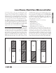
Low-Power, Dual-Core Microcontroller MAXQ3108 Pin Configuration TOP VIEW P2.0/MDIN2P/MOSI 1 28 P2.1/MDIN2N/MISO P0.0/TXD0/INT0 2 27 P2.2/SCLK/CLKO P0.1/RXD0/INT1 3 26 P2.3/MDIN0N/SSEL P2.4/MDIN0P P0.2/MDIN1N/T2P/INT2 4 25 P0.3/MDIN1P/T2PB/INT3 5 24 P1.6/RST P0.4/SDA/INT4 6 23 P0.6/TXD1/INT6 P0.5/SCL/INT5 7 22 P0.7/RXD1/INT7 P2.5/CF1 8 21 VDD MAXQ3108 P2.6/CF2 9 20 REGOUT P1.0/TMS/INT8 10 19 VBAT P1.1/TCK/INT9 11 18 P1.5/TBA P1.2/TDI/INT10 12 17 GND P1.