EMBEDDED AND NETWORK COMPUTING TECHNOLOGIES USERS GUIDE QIL-A9260 Calao Systems 334 rue des Vingt Toises Le MagistèreII 38950 Saint Martin Le Vinoux France Phone = +33 (0)4 76 56 38 05 Fax = +33 (0)4 76 56 38 06 E-mail = sales@calao-systems.com = support@calao-systems.
TABLE OF CONTENTS Section 1...............................................................................................................................................2 1.Overview.......................................................................................................................................3 1.1.Scope.....................................................................................................................................3 1.2.Synoptic..................................
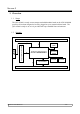
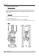
SECTION 1 1. Overview 1.1. Scope The QIL-A9260 is a ready-to-run compact embedded module based on the AT91SAM9260 processor. It has been designed to be easily plugged on your customized base board. The QIL-A9260 is ready to use as it is provided with a pre-installed linux environment. 50 pin expansion connector µSD 1.2.
1.3.
SECTION 2 1. Setting Up the QIL-A9260 1.1. Electrostatic Warning The QIL-A9260 board is shipped in protective anti-static packaging. The board must not be subjected to high electrostatic potentials. A grounding strap or similar protective device should be worn when handling the board. Avoid touching the component pins or any other metallic element. 1.2. Requirements In order to use the QIL-A9260 module, the following items are needed: ● ● ● The QIL-A9260 module itself.
1.4. Powering Up the Board The QIL-A9260 is supplied by the motherboard. It only needs a +3.3V power supply. 1.5. Getting Started The QIL-A9260 key is delivered with a pre-installed U-Boot boot loader and an Embedded Linux operating system. Uboot and linux kernel are stored in the NAND Flash memory. You can update your board by downloading all the available sources and tools on the calao website www.calao-systems.com in order to adapt your system to your needs.
SECTION 3 1.
Reset Controller (RSTC) ✔ Based on a Power-on Reset Cell, Reset Source Identification and Reset Output Control Clock Generator (CKGR) Selectable 32768Hz Low-power Oscillator or Internal Low Power RC Oscillator on Battery Backup Power Supply, Providing a Permanent Slow Clock ✔ 3 to 20 MHz On-chip Oscillator, One up to 240 MHz PLL and One up to 130 MHz PLL ✔ Power Management Controller (PMC) ✔ Very Slow Clock Operating Mode, Software Programmable Power Optimization Capabilities ✔ Two Programmable Ex
Four Universal Synchronous/Asynchronous Receiver Transmitters (USART) ✔ Individual Baud Rate Generator, IrDA® Infrared Modulation/Demodulation, Manchester Encoding/Decoding ✔ Support for ISO7816 T0/T1 Smart Card, Hardware Handshaking, RS485 Support ✔ Full Modem Signal Control on USART0 Two 2-wire UARTs Two Master/Slave Serial Peripheral Interfaces (SPI) ✔ 8- to 16-bit Programmable Data Length, Four External Peripheral Chip Selects ✔ Synchronous Communications Two Three-channel 16-bit Timer/Co
1.1. Microcontroller 1x LFBGA 217-ball fitted on board 1.2.
Bank Start address Size Description Internal memories 0x00000000 256Mbytes EBI CS0 0x10000000 256Mbytes Available on MB EBI CS1 (SDRAMC) 0x20000000 64Mbytes Soldered SDRAM EBI CS2 0x30000000 Not available EBI CS3 (NAND) 0x40000000 256Mbytes Soldered NAND Flash EBI CS4 0x50000000 256Mbytes Available on MB EBI CS5 0x60000000 Not available EBI CS6 0x70000000 256Mbytes Available on MB EBI CS7 0x80000000 256Mbytes Available on MB 1.3.
SECTION 4 1. Configuration 1.1. Solder pads configuration Designation Default setting JP2 closed Feature NAND chip select opened: Nand chip select not wired closed: Nand chip select wired JP3 closed Phy IRQ line connection JP4 closed User Push-button connection JP5 1-2 VDDBU 1-2: 1.8V from the low dropout voltage regulator 2-3: VBAT signal on J1.
1.2. Ethernet The DP83848C is wired in RMII mode. 1.3. Expansion connector ● Pin expansion connector (J1) Description Pin Description 1 +3.
1.4. QIL-128 pins connector J3 Pin Description Pin Description 1 +3.3V 2 GND 3 A0 4 D0 5 A1 6 D1 7 A2 8 D2 9 A3 10 D3 11 A4 12 D4 13 A5 14 D5 15 A6 16 D6 17 A7 18 D7 19 GND 20 +3.3V 21 A8 22 D8 23 A9 24 D9 25 A10 26 D10 27 A11 28 D11 29 A12 30 D12 31 A13 32 D13 33 A14 34 D14 35 A15 36 D15 37 +3.
J4 Pin Description Pin Description 1 +3.
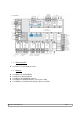
SECTION 5 1. Schematics 1.1.
Datasheet USG-00006-A01 17/20
Datasheet USG-00006-A01 18/20
Datasheet USG-00006-A01 19/20
SECTION 6 1. Errata SECTION 7 1. Revision History 1.1. Revision History Date Version Remarks 2007-09-18 A01 first version SECTION 8 1. COPYRIGHT Notice: The products specifications provided in this datasheet are subject to change without notice. ©2007 CALAO SYSTEMS-All Rights Reserved. The CALAO SYSTEMS logo is a registered trademark of CALAO SYSTEMS. All other names are the property of their respective owners.