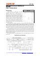
RF12B RF12B Universal ISM Band FSK Transceiver RF12B DESCRIPTION Hope’s multi-channel RF12B FSK is a single transceiver chip, designed low for power, use in applications requiring FCC or ETSI conformance for unlicensed use in the 433, 868 and 915 MHz bands. The RF12B transceiver produces a flexible, low cost, and highly integrated solution that does not require production alignments.
RF12B FEATURES z Fully integrated (low BOM, easy design-in) z No alignment required in production z Fast-settling, programmable, high-resolution PLL synthesizer z Fast frequency-hopping capability z High bit rate (up to 115.
RF12B DETAILED FEATURE-LEVEL DESCRIPTION The RF12B FSK transceiver is designed to cover the unlicensed frequency bands at 433, 868 and 915 MHz. The device facilitates compliance with FCC and ETSI requirements. The receiver block employs the Zero-IF approach with I/Q demodulation, allowing the use of a minimal number of external components in a typical application.
RF12B Data Filtering and Clock Recovery Output data filtering can be completed by an external capacitor or by using digital filtering according to the final application. Analog operation: The filter is an RC type low-pass filter followed by a Schmitt-trigger (St). The resistor (10 kOhm) and the St are integrated on the chip. An (external) capacitor can be chosen according to the actual bit rate. In this mode, the receiver can handle up to 256 kbps data rate.
RF12B The RF12B has a single-pin crystal oscillator circuit, which provides a 10 MHz reference signal for the PLL. To reduce external parts and simplify design, the crystal load capacitor is internal and programmable. Guidelines for selecting the appropriate crystal can be found later in this datasheet. The transceiver can supply a clock signal for the microcontroller; so accurate timing is possible without the need for a second crystal.
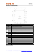
RF12B PACKAGE PIN DEFINITIONS Pin type key: D=digital, A=analog, S=supply, I=input, O=output, IO=input/output Pin 1 2 3 4 5 6 Name SDI SCK nSEL SDO nIRQ FSK DATA Type DI DI DI DO DO DI DO nFFS DI 7 8 9 10 11 12 13 14 15 16 Function Data input of the serial control interface (SPI compatible) Clock input of the serial control interface Chip select input of the serial control interface (active low) Serial data output with bus hold Interrupt request output (active low) Transmit FSK data input (internal pu
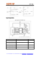
RF12B PIN6(FSK/DATA/nFFS) internal structure PIN10(nRES) internal structure Typical Application Typical application with FIFO usage Pin 7 Pin 6 Transmit mode TX Data input - nFFS input (TX Data register can be accessed) - el=0 in Configuration Setting Command Transmit mode el=1 in Configuration Setting Command Receive mode RX Data output RX Data clock output nFFS input (RX Data FIFO can be accessed) FFIT output ef=0 in Configuration Setting Command Receive mode ef=1 in Configuration Setting Co
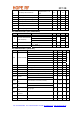
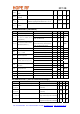
RF12B GENERAL DEVICE SPECIFICATION All voltages are referenced to Vss, the potential on the ground reference pin VSS. Absolute Maximum Ratings (non-operating) Symbol Parameter Min Max Units Vdd Positive supply voltage -0.5 6 V Vin Voltage on any pin (except RF1 and RF2) -0.5 V Voc Voltage on open collector outputs (RF1, RF2) -0.5 Iin Input current into any pin except VDD and VSS -25 Vd d +0.5 Vd d +1.
RF12B Vlb Vlba Vil Vih Low battery detect threshold Programmable in 0.1V steps 2.2 Low battery detection accuracy 0 Digital input low level voltage 3.7 V 5 % * V 0.3 Vdd * Digital input high level voltage 0.7 Vdd V Iil Digital input current Vil = 0 V -1 1 µA Iih Digital input current Vih = Vdd , Vdd = 3.8 V -1 1 µA 0.4 V Vol Digital output low level Iol = 2 mA Voh Digital output high level Ioh = -2 mA Vdd -0.
RF12B CARSSI Filter capacitor for 1 ARSSI nF RSSI programmable RSstep RSresp 6 dB 500 us level steps DRSSI response Until the RSSI signal goes high after the input signal time exceeds the preprogrammed limit CARRSI = 4.7 nF Receiver spurious Psp_rx -60 dBm emission AC Characteristics (Transmitter) Symbol Parameter IOUT Conditions/Notes Psp Pharm Co Qo Lout 6 Max. output power delivered to 50 In 433 MHz band 7 In 868 / 915 MHz bands 5 network (Note 4) Pout Typ Max 0.
RF12B AC Characteristics (Others) Symbol Cxl Parameter Conditions/Notes Crystal load capacitance, Programmable in 0.5 pF steps, tolerance see crystal selection guide +/- 10% tPOR Internal POR timeout tPBt Wake-up timer clock period Cin, D tr, f Min Typ Max Units 8.5 After Vdd has reached 90% of final value (Note 9) 0.95 Calibrated every 30 seconds Digital input capacitance Digital output rise/fall time 15 pF pure capacitive load 16 pF 100 ms 1.
RF12B CONTROL INTERFACE Commands to the transmitter are sent serially. Data bits on pin SDI are shifted into the device upon the rising edge of the clock on pin SCK whenever the chip select pin nSEL is low. When the nSEL signal is high, it initializes the serial interface. All commands consist of a command code, followed by a varying number of parameter or data bits. All data are sent MSB first (e.g. bit 15 for a 16-bit command). Bits having no influence (don’t care) are indicated with X.
RF12B Control Commands Control Command Related Parameters/Functions 1 Configuration Setting Command 2 Power Management Command 3 4 Related control bits Frequency band, crystal oscillator load capacitance, el, ef, b1 to b0, x3 to x0 baseband filter bandwidth, etc.
RF12B 2.
RF12B 3. Frequency Setting Command bit 15 14 13 12 11 10 9 8 7 6 5 4 3 2 1 0 POR 1 0 1 0 f11 f10 f9 f8 f7 f6 f5 f4 f3 f2 f1 f0 A680h The 12-bit parameter F (bits f11 to f0) should be in the range of 96 and 3903. When F value sent is out of range, the previous value is kept. The synthesizer band center frequency f0 can be calculated as: f0 = 10 * C1 * (C2 + F/4000) [MHz] The constants C1 and C2 are determined by the selected band as: 4.
RF12B Bits 7-5 (i2 to i0): Receiver baseband bandwidth (BW) select: i2 i1 i0 BW [kHz] 0 0 0 reserved 0 0 1 400 0 1 0 340 0 1 1 270 1 0 0 200 Bits 2-0 (r2 to r0): RSSI detector threshold: 1 0 1 134 r2 r1 r0 RSSIsetth [dBm] 1 1 0 67 0 0 0 -103 1 1 1 reserved 0 0 1 -97 0 1 0 -91 Bits 4-3 (g1 to g0): LNA gain select: 0 1 1 -85 g1 g0 relative to maximum [dB] 1 0 0 -79 0 0 0 1 0 1 -73 0 1 -6 1 1 0 Reserved 1 0 -14 1 0 1 Reserved
RF12B Bits 4 (s): Select the type of the data filter: s Filter Type 0 Digital filter 1 Analog RC filter Digital: This is a digital realization of an analog RC filter followed by a comparator with hysteresis. The time constant is automatically adjusted to the bit rate defined by the Data Rate Command. Note: Bit rate can not exceed 115 kbps in this mode. Analog RC filter: The demodulator output is fed to pin 7 over a 10 kOhm resistor.
RF12B Bit 1 (ff): FIFO fill will be enabled after synchron pattern reception. The FIFO fill stops when this bit is cleared. Bit 0 (dr): Disables the highly sensitive RESET mode. If this bit is cleared, a 500 mV glitch in the power supply may cause a system reset. Note: To restart the synchron pattern recognition, bit 1 should be cleared and set. 8.
RF12B Bit 3 (st): Strobe edge, when st goes to high, the actual latest calculated frequency error is stored into the offset register of the AFC block. Bit 2 (fi): Switches the circuit to high accuracy (fine) mode. In this case, the processing time is about twice longer, but the measurement uncertainty is about the half. Bit 1 (oe): Enables the frequency offset register. It allows the addition of the offset register to the frequency control word of the PLL.
RF12B only one transmitter. After a complete measuring cycle, the measured value is kept independently of the state of the VDI signal. 11.
RF12B Bit 4 (lpx): When this bit is set, low power mode of the crystal oscillator is selected. lpx Crystal start-up time (typ) Power consumption (typ) 0 1 ms 620 uA 1 2 ms 460 uA (Typ conditions: Top = 27 oC; Vdd = Voc = 2.7 V, Crystal ESR = 30 Ohm) We have test that the default value(0) of bit lpx in PLL setting command will lead to part of RF12B/RFM12B's oscillator fail. it should be set 1 in software manually. for example, use 0xCC77 instead of 0xCC67 as PLL setting command.
RF12B bit 15 14 13 12 11 10 9 8 7 6 5 4 3 2 1 0 POR 1 1 0 0 1 0 0 r0 d6 d5 d4 d3 d2 d1 d0 en C80Eh With this command, Low Duty-Cycle operation can be set in order to decrease the average power consumption in receiver mode. The time cycle is determined by the Wake-Up Timer Command. The Duty-Cycle can be calculated by using (d6 to d0) and M. (M is parameter in a Wake-Up Timer Command.) Duty-Cycle= (D * 2 +1) / M *100% Bit 0 (en): Enables the Low Duty-Cycle Mode.
RF12B 1 0 1 3.33 1 1 0 5 1 1 1 10 The low battery detector and the clock output can be enabled or disabled by bits eb and dc, respectively, using the Power Management Command. 17. Status Read Command The read command starts with a zero, whereas all other control commands start with a one.
RF12B in the AFC Control Command (bit 0). TX REGISTER BUFFERED DATA TRANSMISSION In this operating mode (enabled by bit el, in the Configuration Control Command) the TX data is clocked into one of the two 8-bit data registers. The transmitter starts to send out the data from the first register (with the given bit rate) when bit et is set with the Power Management Command. The initial value of the data registers (AAh) can be used to generate preamble.
RF12B Note: The content of the data registers are initialized by clearing bit et. RX FIFO BUFFERED DATA READ In this operating mode, incoming data are clocked into a 16 bit FIFO buffer. The receiver starts to fill up the FIFO when the Valid Data Indicator (VDI) bit and the synchron pattern recognition circuit indicates potentially real incoming data. This prevents the FIFO from being filled with noise and overloading the external microcontroller.
RF12B Polling Mode: When nFFS signal is low the FIFO output is connected directly to the SDO pin and its content can be clocked out by the SCK. Set the FIFO IT level to 1. In this case, as long as FFIT indicates received bits in the FIFO, the controller may continue to take the bits away. When FFIT goes low, no more bits need to be taken. An SPI read command is also available to read out the content of the FIFO.
RF12B 15 8 8 30 15 15 315 MHz 30 don't use 45 60 7 30 75 50 90 105 75 100 120 100 433 MHz don't use 5 20 30 50 75 75 868 MHz 915 MHz don't use don't use 3 3 10 10 20 15 25 30 25 30 40 40 433 MHz 868 MHz 915 MHz Bit Rate: Bit Rate: 50 25 25 70 30 30 80 40 40 100 100 50 60 50 50 Deviation [+/- kHz] 38.4 kbps Deviation [+/- kHz] 115.
RF12B Note: • LNA gain maximum, filter bandwidth 67 kHz, data rate to 9.6 kbps, AFC switched off, FSK deviation +/- 45 kHz, Vdd = 2.7 V • Measured according to the descriptions in the ETSI Standard EN 300 220-1 v2.1.1 (2006-01 Final Draft), section 9 • The ETSI limit in the figure is drawn by taking 109dBm typical sensitivity into account Phase Noise Performance in the 915 MHz (Green) 868 MHz (Red) and 433 MHz (Blue) Bands: Tel: +86-755-86096587 Fax: +86-755-86096602 E-mail: sales@hoperf.
RF12B (Measured under typical conditions: Top = 27 oC; Vdd = Voc = 2.7 V) BER Curves in 433 MHz Band: BER Curves in 868 MHz Band: Tel: +86-755-86096587 Fax: +86-755-86096602 E-mail: sales@hoperf.com http://www.hoperf.
RF12B The table shows the optimal receiver baseband bandwidth (BW) and transmitter deviation frequency (δ fFSK) selection for different data rates. 1.2 kbps 2.4 kbps 4.8 kbps 9.6 kbps BW=67 kHz BW=67 kHz BW=67 kHz BW=67 kHz 19.2 kbps 38.4 kbps 57.6 kbps 115.2 kbps BW=67 kHz BW=134 kHz BW=134 kHz BW=200 kHz δfFSK =45 kHz δfFSK =45 kHz δfFSK =45kHz δfFSK =45 kHz δfFSK =45 kHz δfFSK =90 kHz δfFSK =90 kHz δfFSK =120 kHz Receiver Sensitivity over Ambient Temperature (433 MHz, 9.
RF12B (868 MHz, 9.6 kbps, δ fFSK: 45 kHz, BW: 67 kHz): Tel: +86-755-86096587 Fax: +86-755-86096602 E-mail: sales@hoperf.com http://www.hoperf.
RF12B REFERENCE DESIGNS Schematic PCB layout Top view Bottom view Tel: +86-755-86096587 Fax: +86-755-86096602 E-mail: sales@hoperf.com http://www.hoperf.
RF12B SGS Reports Tel: +86-755-86096587 Fax: +86-755-86096602 E-mail: sales@hoperf.com http://www.hoperf.
RF12B Tel: +86-755-86096587 Fax: +86-755-86096602 E-mail: sales@hoperf.com http://www.hoperf.
RF12B RF12B BONDING DIAGRAM Pad Opening: 85um square, except 76um octagon pads (AN1, AN2) Die Size: 2750 X 3315 um Tel: +86-755-86096587 Fax: +86-755-86096602 E-mail: sales@hoperf.com http://www.hoperf.
RF12B This document may contain preliminary information and is subject to change by Hope Microelectronics without notice. Hope Microelectronics assumes no responsibility or liability for any use of the information contained herein. Nothing in this document shall operate as an express HOPE MICROELECTRONICS CO.,LTD or implied license or indemnity under the intellectual property rights of 4/F, Block B3, East Industrial Area, Hope Microelectronics or third parties.