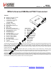
RF22 Version: 0.1 Date: 12/23/2008 RF22 Universal ISM Band FSK Transceiver Features z z z z z z z z z z z z z z z z z z z z z z z z Frequency range = 240–930 MHz Sensitivity = –118dBm +20 dBm Max Output Power Configurable +11 to +20 dBm Low Power Consumption 18.5 mA receive 27mA @ +11dBm Data Rate = 1 to 128kbps Power Supply = 1.8 to 3.
RF22 Version: 0.
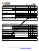
RF22 Version: 0.1 Date: 12/23/2008 Table2. Synthesizer AC Electrical Characteristics1 Parameter Synthesizer Frequency Range 2 Synthesizer Frequency Resolution Reference Frequency Reference Frequency Input Level Synthesizer Settling Time Residual FM tLOCK ΔFRMS 2 Phase Noise 2 2 Symbol FSYNTH-LB FSYNTH-HB FRES-LB FRES-HB fREF fREF_LV LΦ(fM) 2 Spurious Emissions POB-TX1 POB-TX2 2 Conditions Low Band High Band Low Band High Band fcrystal / 3 When using reference frequency instead of crystal.
RF22 Version: 0.1 Date: 12/23/2008 Table4. Transmitter AC Electrical Characteristics1 Parameter TX Frequency Range 2 2 FSK Modulation Data Rate 2 OOK Modulation Data Rate 2 Modulation Deviation Modulation Deviation Resolution 2 Output Power Range 2 TX RF Output Steps 2 TX RF Output Level Variation vs. Voltage 2 TX RF Output Level Variation vs. Temperature 2 TX RF Output Level Variation vs.
RF22 Version: 0.1 Date: 12/23/2008 Table7. GPIO Specifications (GPIO_0, GPIO_1, and GPIO_2) Parameter Rise Time Fall Time Input Capacitance Logic High Level Input Voltage Logic Low Level Input Voltage Input Current Input Current If Pullup is Activated Symbol Conditions TRISE 0.1 x VDD to 0.9 x VDD, CL= 10 pF, DRV<1:0>=HH TFALL 0.9 x VDD to 0.
RF22 Version: 0.1 Date: 12/23/2008 Test Notes: All electrical parameters with Min/Max values are guaranteed by one (or more) of the following test methods. Electrical parameters shown with only typical values are not guaranteed. ■ Guaranteed by design and/or simulation but not tested. ■ Guaranteed by Engineering Qualification testing at Extreme Test Conditions. ■ Guaranteed by 100% Production Test Screening at Production Test Conditions. 2.
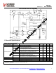
RF22 Version: 0.1 16 nIRQ nSEL 17 18 XIN RF22 C8 13 SCLK GP3 SDI GP4 SDO GP5 microcontroller VDD_D 10 9 12 11 GND_D VR _DI G 1u L4 14 3 RXn 4 VR_IF 5 C10 15 2 RXp 8 C4 VDD GP1 GP2 GPI O2 C1 GPI O1 C2 1 6 C3 TX 20 L1 VDD_RF L3L2 ADC_REF TR & ANT-DIV Switch XOUT 1u SDN 100n X1 30MHz C8 19 100p C7 7 C6 GPI O0 supply voltage Date: 12/23/2008 C9 1u 1u C5 VSS Programmable load capacitors for X1 are integrated.
RF22 ~1ms PLL TS PLL T0 XTAL Settling Time PLL C AL TX Packet P A RAMP D OWN PLLTS PRE P A R AMP P A R AMP UP TXMOD DEL AY XTAL Settling Time PLL T0 PLL CAL Version: 0.1 Date: 12/23/2008 RX Packet Figure2. Configurable 0~310us, Recommended 100us 45us, may be skiped Configurable 0~70us, Default=20us 1.5Bits@DR 6us, Fixed Configurable 5~20us, Recommended 5us Configurable 0~310us, Recommended 100us 45us, may be skiped Configurable 0~70us, Default=20us ~1ms TX Timing. Figure3.
RF22 Version: 0.1 Date: 12/23/2008 To read back data from the RF22, the R/W bit must be set to 0 followed by the 7-bit address of the register from which to read. The 8 bit DATA field following the 7-bit ADDR field is ignored when R/W = 0. The next eight positive edge transitions of the SCLK signal will clock out the contents of the selected register. The data read from the selected register will be available on the SDO output pin. The READ function is shown in Figure 5.
RF22 Version: 0.1 Date: 12/23/2008 The output of the LPLDO is internally connected in parallel to the output of the main digital regulator (and is available externally at the VR_DIG pin); this common digital supply voltage is connected to all digital circuit blocks, including the digital modem, crystal oscillator, and SPI and register space. The LPLDO has extremely low quiescent current consumption but limited current supply capability; it is used only in the IDLE-STANDBY and IDLE-SLEEP modes.
RF22 Version: 0.1 Date: 12/23/2008 3.2.2.2. SLEEP Mode In SLEEP mode the LPLDO is enabled along with the Wake-Up-Timer, which can be used to accurately wake-up the radio at specified intervals. See "8.6. Wake-Up Timer" on page 62 for more information on the Wake-Up-Timer. Sleep mode is entered by setting enwt=1 (40h) in "Register 07h. Operating Mode and Function Control 1". If an interrupt has occurred (i.e.
RF22 Version: 0.1 Date: 12/23/2008 IDLE modes to the RX state. The following sequence of events will occur automatically to get the chip into RX mode when going from STANDBY mode to RX mode by setting the rxon bit: 1. Enable the Main Digital LDO and the Analog LDOs. 2. Start up crystal oscillator and wait until ready (controlled by timer). 3. Enable PLL. 4. Calibrate VCO (this action is skipped when the vcocal bit is “0”; default value is “1”). 5.
RF22 Version: 0.1 Date: 12/23/2008 setting the vcocal bit. The 32.768 kHz RC oscillator is also automatically calibrated but the calibration may also be forced. The enrcfcal will enable the RC Fine Calibration which will occur every 30 seconds. The rccal bit will force a complete calibration of the RC oscillator which will take approximately 2 ms. The PLL T0 time is to allow for bias settling of the VCO, the default for this should be adequate.
RF22 Version: 0.1 Date: 12/23/2008 Table12. Frequency Band Selection fb[4:0] Value N 0 1 2 3 4 5 6 7 8 9 10 11 12 13 14 15 16 17 18 19 20 21 22 23 24 25 26 27 28 29 30 31 32 33 34 35 36 37 38 39 40 41 42 43 44 45 46 47 hbsel=0 240-249.9MHz 250-259.9MHz 260-269.9MHz 270-279.9MHz 280-289.9MHz 290-299.9MHz 300-309.9MHz 310-319.9MHz 320-329.9MHz 330-339.9MHz 340-349.9MHz 350-359.9MHz 360-369.9MHz 370-379.9MHz 380-389.9MHz 390-399.9MHz 400-409.9MHz 410-419.9MHz 420-429.9MHz 430-439.9MHz 440-449.
RF22 Version: 0.1 Date: 12/23/2008 3.2.9.3. Automatic Frequency Change If registers 79h or 7Ah are changed in either TX or RX mode, then the state machine will automatically transition the chip back to tune, change the frequency, and automatically go back to either TX or RX. This feature is useful to reduce the number of SPI commands required in a Frequency Hopping System. This in turn reduces microcontroller activity, reducing current consumption. 3.2.9.4.
RF22 Version: 0.1 Date: 12/23/2008 mode the fo[9:0] register should be set to 360h. When AFC is enabled the same registers can be used to read the offset value as automatically obtained by the AFC. Add 73 74 R/W R/W R/W Function/Description Frequency Offset Frequency Offset D7 fo[7] D6 fo[6] D5 fo[5] D4 fo[4] D3 fo[3] D2 fo[2] D1 fo[1] fo[9] D0 fo[0] fo[8] POR Def. 00h 00h Notes 73 3.2.9.6.
RF22 Version: 0.1 Add 1D R/W R/W Function/Description AFC Loop Gearshift Override D7 afcbd D6 enafc D5 afcgearh[2] D4 afcgearh[1] D3 afcgearh[0] D2 afcgearl[2] Date: 12/23/2008 D1 afcgearl[1] D0 afcgearl[0] POR Def. 40h 3.2.10. TX Data Rate Generator The data rate is configurable between 1–128 kbps. For data rates below 30 kbps the ”txdtrtscale” bit in register 70h should be set to 1. When higher data rates are used this bit should be set to 0.
RF22 Version: 0.1 Date: 12/23/2008 4.2. Modulation Data Source The RF22 may be configured to obtain its modulation data from one of three different sources: FIFO mode, Direct Mode, and from a PN9 mode. Furthermore, in Direct Mode, the TX modulation data may be obtained from several different input pins. These options are set through the dtmod[1:0] field in "Register 71h. Modulation Mode Control 2".
RF22 Version: 0.1 Date: 12/23/2008 nSEL nIRQ XOUT XIN SDN nIRQ SCLK VDD_RF TX RF22 RXp MOSI SDO MISO VR_DIG GND_DIG GPIO_2 VR_IF GPIO_1 VDD_DIG GPIO_0 SCK SDI RXn ADC_REF Matching nSEL uC Direct synchronous modulation . Full control over the standard SPI & using interrupt. Bitrate clock and modulation via GPIO's. GPIO configuration GP0 : power-on-reset (default) GP1 : TX DATA clock output GP2 : TX DATA input MOD DATACLK nRES DataCLK MOD(Data) Figure11.
RF22 Version: 0.1 Date: 12/23/2008 nSEL nIRQ XOUT XIN SDN nIRQ SCLK VDD_RF SCK VDD_DIG VR_IF GND_DIG uC VR_DIG MISO RXn GPIO_2 MOSI GPIO_1 SDI SDO ADC_REF TX RXp GPIO_0 Matching nSEL FIFO mode utilizing internal packet handler. Data loaded/ read through SPI into FIFO . GPIO configuration Not Utilized Figure13. FIFO Mode Example 5. Internal Functional Blocks This section provides an overview some of the key blocks of the internal radio architecture. 5.1.
RF22 Version: 0.1 Date: 12/23/2008 RX Demodulation AGC Preamble Detector Invalid Preamble Detector Radio Signal Strength Indicator (RSSI) Automatic Frequency Compensation (AFC) Packet Handling including EZMacTM features Cyclic Redundancy Check (CRC) The digital Channel Filter and Demodulator are optimized for ultra low power consumption and are highly configurable. Supported modulation types are GFSK, FSK, and OOK.
RF22 Version: 0.1 Date: 12/23/2008 rate can be programmed between 1–128 kbps, and the frequency deviation can be programmed between ±1–160 kHz. These parameters may be adjusted via registers as shown in "3.2.9. Frequency Control" on page 26. TX Fref=10M PFD CP Selectable Divider LPF RX VCO N TX Modulation DeltaSigma Figure14. PLL Synthesizer Block Diagram The reference frequency to the PLL is 10 MHz. The PLL utilizes a differential L-C VCO, with integrated on-chip spiral inductors.
RF22 Version: 0.1 Date: 12/23/2008 down to prevent unwanted spectral splatter. The extra output power can allow use of a cheaper smaller antenna, greatly reducing the overall BOM cost. The higher power setting of the chip achieves maximum possible range, but of course comes at the cost of higher TX current consumption. However, depending on the duty cycle of the system the effect on battery life may be insignificant. Contact HopeRF’s Support for help in evaluating this tradeoff.
RF22 Version: 0.1 Date: 12/23/2008 to address 7Fh will write data to the TX FIFO. A burst read from address 7Fh will read data from the RX FIFO. TX FIFORX FIFO RX FIFO Almost Full Threshold TX FIFO Almost Full Threshold TX FIFO Almost Empty Threshold Figure15. FIFO Thresholds The TX FIFO has two programmable thresholds. An interrupt event occurs when the data in the TX FIFO reaches these thresholds. The first threshold is the FIFO Almost Full threshold, txafthr[5:0].
RF22 Version: 0.1 Date: 12/23/2008 "Register 30h. Data Access Control" through "Register 49h. Received Header 1" are used to set the different fields in the packet structure. Automatically adding these fields to the data payload greatly reduces the amount of communication between the microcontroller and the RF22 and therefore also reduces the required computational power of the microcontroller.
RF22 Version: 0.1 Date: 12/23/2008 6.4.2. Packet Handler Enabled When the packet handler is enabled, all the fields of the packet structure need to be configured. If multiple packets are desired to be stored in the FIFO, then there are options available for the different fields that will be stored into the FIFO. Figure 19 demonstrates the options and settings available when multiple packets are enabled. Figure 20 demonstrates the operation of fixed packet length and correct/incorrect packets.
RF22 Version: 0.1 Date: 12/23/2008 Table14. Packet Handler Registers Addr R/W Function/Description D7 D6 D5 D4 D3 D2 D1 D0 POR Def.
RF22 Version: 0.1 Date: 12/23/2008 Manchester Whitening CRC Preamble HEADER/ ADDRESS SYNC PK Length CRC (data only = 1) DATA CRC 6.6. Preamble Detector The RF22 has integrated automatic preamble detection. The preamble length is configurable from 1–256 bytes using the prealen[7:0] field in "Register 33h. Header Control 2" and "Register 34h. Preamble Length", as described in “6.2. Packet Configuration”. The preamble detection threshold, preath[4:0] as set in "Register 35h.
RF22 Version: 0.1 Date: 12/23/2008 The Invalid Preamble Detector issues an interrupt when no valid preamble signal is found. After the receiver is enabled, the Invalid Preamble Detector will be held low for 16 Tb (Tb is the time of the bit duration) to allow the receiver to settle. The 16 Tb is a fixed time which will work with a 4-byte Preamble (or longer) when AFC is enabled, or a 3-byte preamble (or longer) when AFC is disabled.
RF22 Version: 0.1 10 19.2 20 20 38.4 40 40 50 57.6 100 100 125 40 9.6 10 40 19.6 20 40 25 28.8 50 300 125 8.00 1.00 1.00 4.00 1.02 1.00 2.00 1.00 1.00 1.00 6.00 2.00 90 37.7 37.7 95.3 75.2 75.2 112.1 75.2 90 191.5 620.7 335.5 0 0 0 0 0 0 0 0 0 1 1 1 0 1 1 0 0 0 0 0 0 0 0 0 3 1 1 4 1 1 5 1 3 F E 8 190 068 064 0C8 068 064 064 050 045 078 078 060 Date: 12/23/2008 051EC 13A93 147AE 0A3D7 13A93 147AE 147AE 1999A 1D7DC 11111 11111 15555 02B 4EE 521 0A6 4D5 521 291 668 76E 446 0B8 2AD 7.1.1.
RF22 Version: 0.1 Date: 12/23/2008 Table17. Filter Bandwidth Parameters BW [kHz] 2.6 2.8 3.1 3.2 3.7 4.2 4.5 4.9 5.4 5.9 6.1 7.2 8.2 8.8 9.5 10.6 11.5 12.1 14.2 16.2 17.5 18.9 21.0 22.7 24.0 28.2 32.2 34.7 37.7 ndec_exp 1C-[6:4] 5 5 5 5 5 5 5 4 4 4 4 4 4 4 3 3 3 3 3 3 3 2 2 2 2 2 2 2 1 dwn3_bypass 1C-[7] 0 0 0 0 0 0 0 0 0 0 0 0 0 0 0 0 0 0 0 0 0 0 0 0 0 0 0 0 0 filset 1C-[3:0] 1 2 3 4 5 6 7 1 2 3 4 5 6 7 1 2 3 4 5 6 7 1 2 3 4 5 6 7 1 BW [kHz] 41.7 45.2 47.9 56.2 64.1 69.2 75.2 83.2 90.0 95.3 112.
RF22 Version: 0.1 468.4 518.8 577 620.7 1 1 1 1 Date: 12/23/2008 11 12 13 14 The proper settings for ndec[2:0] are listed in Table 19 where Rb is the data rate (Rb) which is doubled when Manchester coding is enabled. Table19. ndec[2:0] Settings Rb(1+ enmanch) [kbps] Min Max 0 1 2 3 8 40 ndec[2:0] 1 2 3 8 40 65 5 4 3 2 1 0 The clock recovery oversampling rate is set via rxosr[10:0] in "Register 20h. Clock Recovery Oversampling Rate" and "Register 21h. Clock Recovery Offset 2".
RF22 Version: 0.1 19.2 20 30 38.4 40 335 335 335 335 335 1 1 1 1 1 1 1 1 1 1 8 8 8 8 8 139 12C 0C8 09C 096 Date: 12/23/2008 068DC 06D3A 0A3D7 0D1B7 0DA74 0D3 0DC 14A 1A6 1B7 Table21.
RF22 Version: 0.1 Date: 12/23/2008 Table22. POR Parameters Parameter Release Reset Voltage Power-On VDD Slope Low VDD Limit Software Reset Pulse Threshold Voltage Reference Slope VDD Glitch Reset Pulse Symbol VRR SVDD VLD TSWRST VTSD K TP Comment Min 0.85 0.03 0.7 50 tested VDD slope region VLD
RF22 Version: 0.1 Date: 12/23/2008 8.3. General Purpose ADC An 8-bit SAR ADC is integrated onto the chip for general purpose use, as well as for digitizing the temperature sensor reading. “Register 0Fh. ADC Configuration,” on page 56 must be configured depending on the use of the GP ADC before use. The architecture of the ADC is demonstrated in Figure 23. First the input of the ADC must be selected by setting the ADCSEL[2:0] depending on the use of the ADC.
RF22 Version: 0.1 3:2 adcref[1:0] 1:0 adcgain[1:0] Date: 12/23/2008 The internal 8 bit ADC input source can be selected as follows: 000: Internal Temperature Sensor 001: GPIO0, single-ended 010: GPIO1, single-ended 011: GPIO2, single-ended 100: GPIO0(+) – GPIO1(–), differential 101: GPIO1(+) – GPIO2(–), differential 110: GPIO0(+) – GPIO2(–), differential 111: GND ADC Reference Voltage Selection. The reference voltage of the internal 8 bit ADC can be selected as follows: 0X: bandgap voltage (1.
RF22 Version: 0.1 Date: 12/23/2008 The gain is different for different VDD dependent references so the reference change has no influence on input range and digital measured values. The differential offset can be coarse compensated by the adcoffs[3:0] bits found in "Register 11h. ADC Value". Fine compensation should be done by the microcontroller software. The main reason for the offset compensation is to shift the negative offset voltage of the bridge sensor to the positive differential voltage range.
RF22 Version: 0.1 Date: 12/23/2008 Bit D7 D6 D5 D4 D3 D2 D1 D0 Name tsrange[1:0] entoff envbgcal vbgcal[3:0] Type R/W R/W R/W R/W Reset value = 00100000 Bit Name Function 7:6 tsrange[1:0] Temperature Sensor Range Selection. (FS range is 0..1024 mV) o o o 00: –64 C~64 C (full operating range), with 0.5 C resolution (1 LSB in the 8 bit ADC) o o o 01: –64 C ~192 C, with 1 C resolution (1 LSB in the 8 bit ADC) o o o 11: 0 C~128 C, with 0.
RF22 Version: 0.1 Date: 12/23/2008 8.5. Low Battery Detector A low battery detector (LBD) with digital read-out is integrated into the chip. A digital threshold may be programmed into the lbdt[4:0] field in "Register 1Ah. Low Battery Detector Threshold". When the digitized battery voltage reaches this threshold an interrupt will be generated on the nIRQ pin to the microcontroller. The microcontroller will then need to verify the interrupt by reading "Register 03h. Interrupt/Status 1" and "Register 04h.
RF22 Version: 0.1 Date: 12/23/2008 Use of the D variable in the formula is only necessary if finer resolution is required than the R value gives.
RF22 TLDC = ldc[7 : 0]× 2 × (R − D ) × 32 ms 32.768 Version: 0.1 Date: 12/23/2008 Figure28. Low Duty Cycle Mode 8.8. GPIO Configuration Three general purpose IOs (GPIOs) are available. Numerous functions such as specific interrupts, TRSW control, Antenna Diversity Switch control, Microcontroller Output, etc. can be routed to the GPIO pins as shown in the tables below. When in Shutdown mode all the GPIO pads are pulled low.
RF22 Version: 0.
RF22 Version: 0.1 Date: 12/23/2008 obtain good antenna selection is 8 bytes. A special antenna diversity algorithm (antdiv[2:0] = 110 or 111) is included that allows for shorter preamble for TDMA like systems where the arrival of the packet is synchronized to the receiver enable. The recommended preamble length to obtain good antenna selection for synchronized mode is 4 byte.
RF22 Version: 0.1 Date: 12/23/2008 RSSI vs Input Power 250 200 RSSI 150 100 50 0 -120 -100 -80 -60 -40 -20 0 20 In Pow [dBm] Figure 30. RSSI Value vs. Input Power 8.12. Analog and Digital Test Bus A differential analog test bus (ATB) is integrated into the RF22 to provide access to internal analog signals for debugging and test purposes. The available signals are shown in Table 25 and are controlled by the atb[4:0] field in "Register 50h. Analog Test Bus Select".
RF22 Version: 0.1 30 31 RFBG VCOBG Date: 12/23/2008 RFVREG VCOVREG A digital test bus (DTB) is also integrated into the digital portion of the design. The DTB may be configured for output on the GPIOs. For configuring of the GPIO see registers 0Bh-0Dh. The available digital test points are controlled by the dtb[4:0] field in "Register 51h. Digital Test Bus Select". Table 26.
RF22 Version: 0.1 47 Date: 12/23/2008 prog_req mod_en freq. channel update request freq_err wrong freq. indication dsm_rst_s_n dsm sync. reset 48 modulator enable tx_rdy TX ready tx_clk TX clock from NCO 49 dp_rx_en packet handler (RX) enable prea_valid valid preamble pk_srch packet is being searched 50 pk_srch packet is being searched sync_ok rx_data packet handler RX data input 51 pk_rx packet is being received sync_ok pk_valid valid packet received 52 sync_ok sync.
RF22 Version: 0.1 Date: 12/23/2008 9. Reference Design Tel: +86-755-82973805 Fax: +86-755-82973550 E-mail: sales@hoperf.com http://www.hoperf.
RF22 Version: 0.1 Date: 12/23/2008 Tel: +86-755-82973805 Fax: +86-755-82973550 E-mail: sales@hoperf.com http://www.hoperf.
RF22 Version: 0.1 Date: 12/23/2008 10. Measurement Results Adjacent Channel Selectivity at 50 kbps Measured at RX SMA Connector Input Sensitivity vs. Data Rate Measured at RX SMA Connector Input -100 dBm 10 dB AGC Enabled 0 dB -104 dBm -10 dB -106 dBm C/I -108 dBm -110 dBm -20 dB -112 dBm -30 dB -114 dBm -40 dB -116 dBm -50 dB -118 dBm -120 dBm 1 kbps -60 dB 10 kbps 100 kbps 1000 kbps -1.00 MHz Data Rate -0.75 MHz -0.50 MHz -0.25 MHz 0.00 MHz 0.25 MHz 0.50 MHz 0.75 MHz 1.
RF22 Version: 0.1 Figure 48. TX Unmodulated Spectrum (917 MHz) Date: 12/23/2008 Figure 49. TX Modulated Spectrum (917 MHz, 40 kbps, 20 kHz Deviation, GFSK) Figure50. Synthesizer Settling Time for 1 MHz Jump Settled within 10 kHz Figure 51. Synthesizer Phase Noise (VCOCURR = 11) 11. Application Notes 11.1. Crystal Selection The recommended crystal parameters are given in Table 30. Table30.
RF22 Version: 0.1 Date: 12/23/2008 11.2. Layout Practice The following are some general best practice guidelines for PCB layout : Bypass capacitors should be placed as close as possible to the pin. z TX/RX matching/layout should mimic reference as much as possible. Failing to do so may cause loss in performance.
RF22 Version: 0.1 Date: 12/23/2008 11.4. Microcontroller Connection If the FIFO is not desired to be used and minimizing microcontroller pins is important in the application then the SPI interface pins may be used in the following fashion to send/read the data from the transceiver. If it is desired to use the chip in this mode, contact customer support for further instructions. Figure54. Microcontroller Connection Tel: +86-755-82973805 Fax: +86-755-82973550 E-mail: sales@hoperf.com http://www.hoperf.
RF22 Version: 0.1 Date: 12/23/2008 12. Reference Material 12.1. Complete Register Table and Descriptions Register 00h. Device Type Code (DT) Bit D7 D6 Name Reserved Type R Reset value = 00001000 Bit Name 7:5 Reserved 4:0 dt[4:0] D5 D4 D3 D2 dt[4:0] R D1 D0 D2 vc[4:0] R D1 D0 D1 D0 Function Reserved. Device Type Code. Indicates if the device is a transmitter, receiver, or a transceiver. RX: 01000 TRX: 00111 Register 01h.
RF22 Version: 0.1 Date: 12/23/2008 Register 03h. Interrupt/Status 1 Bit D7 D6 Name ifferr itxffafull Type R R Reset value = xxxxxxxx Bit Name 7 ifferr 6 itxffafull 5 itxffaem 4 irxffafull 3 iext 2 ipksent 1 ipkvalid 0 icrcerror D5 itxffaem R D4 irxffafull R D3 iext R D2 ipksent R D1 ipkvalid R D0 icrcerror R Function FIFO Underflow/Overflow Error. When set to 1 the TX or RX FIFO has overflowed or underflowed. TX FIFO Almost Full.
RF22 Version: 0.1 Date: 12/23/2008 Table 34. When do the individual Status Bits get Set/Cleared, if not Enabled as an Interrupt? Bit 7 Status Name ifferr 6 itxffafull 5 itxffaem 4 irxffafull 3 2 iext ipksent 1 ipkvalid 0 icrcerror Set/Clear Conditions Set if there is a TX or RX FIFO Overflow or Underflow. It is cleared only by applying FIFO reset to the specific FIFO that caused the condition.
RF22 Version: 0.1 Date: 12/23/2008 Table 35. Interrupt or Status 2 Bit Set/Clear Description Bit 7 Status Name iswdet 6 ipreaval 5 4 3 2 ipreainval irssi iwut ilbd 1 ichiprdy 0 ipor Set/Clear Conditions Goes high once the Sync Word is detected. Goes low once we are done receiving the current packet. Goes high once the preamble is detected. Goes low once the sync is detected or the RX wait for the sync times-out. Self cleaning, user should use this as an interrupt source rather than a status.
RF22 Version: 0.1 Date: 12/23/2008 Register 06h. Interrupt Enable 2 Bit D7 D6 Name enswdet enpreaval Type R R Reset value = 00000011 Bit Name 7 enswdet 6 enpreaval 5 enpreainval 4 enrssi 3 enwut 2 enlbd 1 enchiprdy 0 enpor D5 enpreainval R D4 enrssi R D3 enwut R/W D2 enlbd R/W D1 enchiprdy R/W D0 enpor R/W Function Enable Sync Word Detected. When mpreadet =1 the Preamble Detected Interrupt will be enabled. Enable Valid Preamble Detected.
RF22 Version: 0.1 Date: 12/23/2008 Register 08h. Operating Mode and Function Control 2 Bit D7 D6 Name antdiv[2:0] Type R/W Reset value = 00000000 Bit Name 7:5 antdiv[2:0] 4 rxmpk 3 autotx 2 enldm 1 ffclrrx 0 ffclrtx D5 D4 rxmpk R/W D3 autotx R/W D2 enldm R/W D1 ffclrrx R/W D0 ffclrtx R/W Function Enable Antenna Diversity. The GPIO must be configured for Antenna Diversity for the algorithm to work properly.
RF22 Version: 0.1 Date: 12/23/2008 Register 0Ah. Microcontroller Output Clock Bit D7 Name D6 D5 Reserved Type R Reset value = xx000110 Bit Name 7:6 Reserved 5:4 clkt[1:0] 3 enlfc 2:0 mclk[2:0] D4 D3 clkt[1:0] enlfc R/W R/W D2 D1 D0 mclk[2:0] R/W Function Reserved. Clock Tail. If enlfc = 0 then it can be useful to provide a few extra cycles for the microcontroller to complete its operation.
RF22 Version: 0.
RF22 Version: 0.1 Date: 12/23/2008 Register 0Dh. GPIO Configuration 2 Bit D7 D6 Name gpiodrv2[1:0] Type R/W Reset value = 00000000 Bit Name 7:6 gpiodrv2[1:0] 5 pup2 4:0 gpio2[4:0] D5 pup2 R/W D4 D3 D2 gpio2[4:0] R/W D1 D0 Function GPIO Driving Capability Setting. Pullup Resistor Enable on GPIO2. When set to 1 the a 200 k resistor is connected internally between VDD and the pin if the GPIO is configured as a digital input. GPIO1pin Function Select.
RF22 Version: 0.1 2 dio2 1 dio1 0 dio0 Date: 12/23/2008 Direct I/O for GPIO2. If the GPIO2 is configured to be a direct output then the value on the GPIO pin can be set here. If the GPIO2 is configured to be a direct input then the value of the pin can be read here. Direct I/O for GPIO1. If the GPIO1 is configured to be a direct output then the value on the GPIO pin can be set here. If the GPIO1 is configured to be a direct input then the value of the pin can be read here. Direct I/O for GPIO0.
RF22 Version: 0.1 Reset value = xxxxxxxx Bit Name 7:0 adc[7:0] Date: 12/23/2008 Function Internal 8 bit ADC Output Value. Register 12h. Temperature Sensor Calibration Bit D7 D6 Name tsrange[1:0] Type R/W Reset value = 00100000 Bit Name 7:6 tsrange[1:0] 5 4 3:0 entsoffs entstrim tstrim[3:0] D5 entsoffs R/W D4 entstrim R/W D3 D2 D1 D0 tstrim[3:0] R/W Function Temperature Sensor Range Selection. (FS range is 0..1024 mV) o o o 00: -40 C~64 C (full operating range), with 0.
RF22 Version: 0.1 Date: 12/23/2008 Register 16h. Wake-Up Timer Period 3 Bit D7 D6 D5 D4 D3 Name wtm[7:0] Type R/W Reset value = 00000000 Bit Name Function 7:0 wtm[7:0] Wake Up Timer Mantissa (M) Value*. R-D *Note: The period of the wake-up timer can be calculated as TWUT = (32 x M x2 ) / 32.768 ms. D2 D1 D0 D2 D1 D0 D2 D1 D0 Bit D7 D6 D5 D4 D3 D2 Name ldc[7:0] Type R/W Reset value = 00000000 Bit Name Function 7:0 ldc[7:0] Low-Duty Cycle Mode Duration (LDC)*.
RF22 Version: 0.1 Date: 12/23/2008 *Note: The threshold can be calculated as Vthreshold = (1.675 + LBDT * 50 mV) ±25 mV. Register 1Bh. Battery Voltage Level Bit D7 D6 Name Reserved Type R Reset value = xxxxxxxx Bit Name 7:5 Reserved 4:0 vbat[4:0] D5 D4 D3 D2 vbat[4:0] R D1 D0 Function Reserved. Battery Voltage Level. The battery voltage is converted by a 5 bit ADC. In Sleep Mode the register is updated in every 1 s. In other states it measures continuously. Register 1Ch.
RF22 Version: 0.1 BCRLoopGain = Date: 12/23/2008 crgain 2 crfast Once the preamble is detected, internal state machine automatically shift BCR loop gain to the following: BCRLoopGain = crgain 2 crslow crfast = 3’b000 and crslow = 3’b101 are recommended for most applications. The value of “crslow” should be greater than “crfast”. Register 1Fh.
RF22 Version: 0.1 Date: 12/23/2008 Register 21h. Clock Recovery Offset 2 Bit D7 D6 Name rxosr[10:8] Type R/W Reset value = 00000001 Bit Name 7:5 rxosr[10:8] 4 stallctrl 3:0 ncoff[19:16] D5 D4 stallctrl R/W D3 D2 D1 D0 ncoff[19:16] R/W Function Oversampling Rate. Upper bits. Used for BCR Purposes. NCO Offset. See formula above. Register 22h.
RF22 Version: 0.1 Date: 12/23/2008 Register 26h. Received Signal Strength Indicator Bit D7 Name Type Reset value = 00000000 Bit Name 7:0 rssi[7:0] D6 D5 D4 D3 D2 D1 D0 D2 D1 D0 D3 D2 D1 D0 D3 D2 D1 D0 D1 D0 rssi[7:0] R Function Received Signal Strength Indicator Value. Register 27h. RSSI Threshold for Clear Channel Indicator Bit D7 Name Type Reset value = 00000000 Bit Name 7:0 rssith[7:0] D6 D5 D4 rssith[7:0] R/W D3 Function RSSI Threshold.
RF22 Version: 0.1 3 enpactx 2 encrc 1:0 crc[1:0] Date: 12/23/2008 Enable Packet TX Handling. If FIFO Mode (dtmod=10) is being used automatic packet handling may be enabled. Setting enpactx=1 will enable automatic packet handling in the TX path. Register 30-4D allow for various configurations of the packet structure. Setting enpactx=0 will not do any packet handling in the TX path. It will only transmit what is loaded to the FIFO. CRC Enable.
RF22 Version: 0.1 Date: 12/23/2008 Register 33h. Header Control 2 Bit D7 Name Reserved Type R Reset value = 00100010 Bit Name 7 Reserved 6:4 hdlen[2:0] 3 fixpklen 2:1 synclen[1:0] 0 prealen[8] D6 D5 hdlen[2:0] R/W D4 D3 fixpklen R/W D2 D1 synclen[1:0] R/W D0 prealen[8] R/W Function Reserved. Transmit/Receive Header Length. Length of header used if packet handler is enabled for TX/RX (enpactx/rx). Headers are transmitted/received in descending order.
RF22 Version: 0.1 Date: 12/23/2008 Register 36h. Synchronization Word 3 Bit D7 D6 D5 Name D4 D3 D2 D1 D0 D3 D2 D1 D0 D3 D2 D1 D0 D3 D2 D1 D0 D3 D2 D1 D0 sync[31:24] R/W Type Reset value = 00101101 Bit Name 7:0 sync[31:24] Function Synchronization Word 3. 4th byte of the synchronization word. Register 37h. Synchronization Word 2 Bit D7 Name Type Reset value = 11010100 Bit Name 7:0 D6 D5 D4 sync[23:16] R/W Function Synchronization Word 2.
RF22 Version: 0.1 Date: 12/23/2008 Register 3Bh. Transmit Header 2 Bit D7 D6 D5 Name D3 D2 D1 D0 D3 D2 D1 D0 D3 D2 D1 D0 D3 D2 D1 D0 txhd[23:16] R/W Type Reset value = 00000000 Bit Name 7:0 D4 Function Transmit Header 2. 3rd byte of the header to be transmitted. txhd[23:16] Register 3Ch. Transmit Header 1 Bit D7 Name Type Reset value = 00000000 Bit Name 7:0 D6 D5 D4 txhd[15:8] R/W Function Transmit Header 1. 2nd byte of the header to be transmitted. txhd[15:8] Register 3Dh.
RF22 Version: 0.1 Reset value = 00000000 Bit Name 7:0 Date: 12/23/2008 Function Check Header 3. 4th byte of the check header. chhd[31:24] Register 40h. Check Header 2 Bit D7 Name Type Reset value = 00000000 Bit Name 7:0 chhd[23:16] D6 D5 D4 chhd[23:16] R/W D3 D2 D1 D0 D3 D2 D1 D0 D3 D2 D1 D0 Function Check Header 2. 3rd byte of the check header. Register 41h.
RF22 Version: 0.1 Bit Name 7:0 hden[23:16] Date: 12/23/2008 Function Header Enable 2. 3rd byte of the check header. Register 45h. Header Enable 1 Bit D7 D6 D5 Name D3 D2 D1 D0 D3 D2 D1 D0 D3 D2 D1 D0 D3 D2 D1 D0 D3 D2 D1 D0 hden[15:8] R/W Type Reset value = 00000000 Bit Name 7:0 D4 Function Header Enable 1. 2nd byte of the check header. hden[15:8] Register 46h.
RF22 Version: 0.1 Date: 12/23/2008 Register 4Ah. Received Header 0 Bit D7 Name Type Reset value = 00000000 Bit Name 7:0 rxhd[7:0] D6 D5 D4 D3 D2 D1 D0 D3 D2 D1 D0 rxhd[7:0] R Function Received Header 0. 1st byte of the received header. Register 4Bh. Received Packet Length Bit D7 D6 D5 Name Type Reset value = 11111111 Bit Name 7:0 rxplen[7:0] D4 rxplen[7:0] R Function Length Byte of the Received Packet during fixpklen = 0.
RF22 Version: 0.1 Date: 12/23/2008 Register 51h. Digital Test Bus Select Bit D7 D6 Name Reserved ensctest Type R/W R/W Reset value = 00000000 Bit Name 7 Reserved 6 ensctest 5:0 dtb[5:0] D5 D4 D3 D2 D1 D0 dtb[5:0] R/W Function Reserved. Scan Test Enable. When set to 1 then GPIO0 will be the ScanEn input. Digital Test Bus. GPIO must be configured to Digital Test Mux Output. Table37.
RF22 Version: 0.
RF22 Version: 0.1 Date: 12/23/2008 Register 52h. TX Ramp Control Bit D7 D6 Name Reserved Type R/W Reset value = 00100000 Bit Name 7 Reserved 6:4 txmod[2:0] 3:2 ldoramp[1:0] 1:0 txramp[1:0] D5 txmod[2:0] R/W D4 D3 D2 D1 ldoramp[1:0] R/W D0 txramp[1:0] R/W Function Reserved TX Modulation Delay. The time delay between PA enable and the beginning of the TX modulation to allow for PA ramp-up. It can be set from 0 µs to 28 µs in 4 µs steps. This also works during PA ramp down. TX LDO Ramp Time.
RF22 Version: 0.1 Date: 12/23/2008 Register 55h. Calibration Control Bit D7 D6 Name Reserved xtalstarthalf Type R R/W Reset value = x0x00100 Bit Name 7 Reserved 6 xtalstarthalf 5 adccaldone 4 enrcfcal 3 rccal 2 vcocaldp 1 vcocal 0 skipvco D5 adccaldone R D4 enrcfcal R/W D3 rocal R/W D2 vcocaldp R/W D1 vcocal R/W D0 skipvco R/W Function Reserved. If Set, the Xtal Wake Time Period is Halved. Delta-sigma ADC Calibration Done.
RF22 Version: 0.1 3 2:0 Date: 12/23/2008 Charge Pump DC Offset Only. Charge Pump DC Current Selection. cdconly cdcurr[2:0] Register 58h. Charge Pump Current Trimming/Override Bit D7 Name D6 cpcurr[1:0] Type R/W Reset value = 100xxxxx Bit Name 7:6 cpcurr[1:0] 5 4:0 D5 D4 D3 D2 cpcorrov D1 D0 cporr[4:0] R/W R/W Function Charge Pump Current (Gain Setting). Changing these bits will change the BW of the PLL. The default setting is adequate for all data rates.
RF22 Version: 0.1 6:0 Date: 12/23/2008 VCO Calibration Results. vcocal[6:0] Register 5Ch. Synthesizer Test Bit D7 Name dsmdt Type R/W Reset value = 0x001110 Bit Name 7 dsmdt 6 vcotype 5 4 enoloop dsmod 3:2 dsorder[1:0] 1 0 dsrstmode dsrst D6 vcotype R D5 enoloop R/W D4 dsmod R/W D3 D2 D1 dsrstmode R/W D0 dsrst R/W D3 enbf5 R/W D2 endv32 R/W D1 enbf12 R/W D0 enmx2 R/W D3 enbf3 R/W D2 enbf11 R/W D1 enbf2 R/W D0 pllreset R/W dsorder[1:0] R/W Function Enable DSM Dithering.
RF22 Version: 0.1 0 Date: 12/23/2008 PLL Reset Enable Override. pllreset Register 5Fh. Block Enable Override 3 Bit D7 Name enfrdv Type R/W Reset value = 00000000 Bit Name 7 enfrdv 6 endv31 5 endv2 4 endv1p5 3 dvbshunt 2 envco 1 encp 0 enbg D6 endv31 R/W D5 endv2 R/W D4 endv1p5 R/W D3 dvbshunt R/W D2 envco R/W D1 encp R/W D0 enbg R/W D2 D1 D0 D1 D0 Function Fractional Divider Enable Override. Divider 3_1 Enable Override. Divider 2 Enable Override. Divider 1.5 (div-by-1.5) Enable Override.
RF22 Version: 0.1 1 bufovr 0 enbuf Date: 12/23/2008 Output Buffer Enable Override. If set to 1 then the enbuf bit controls the output buffer. 0: output buffer is controlled by the state machine 1: output buffer is controlled by the enbuf bit Output Buffer Enable. This bit is active only if the bufovr bit is set to 1. Register 63h.
RF22 Version: 0.1 Bit 7 Name enovr 6 5 4 3 2:0 enxtal ents enrc32 Reserved diglvl Date: 12/23/2008 Function Enable Overrides. If high, ovr values are output to the blocks and can enable or disable them, if low, some ovr value can only enable the blocks. Xtal Override Enable Value. Temperature Sensor Enable. 32K Oscillator Enable. Reserved. Digital LDO Level Setting. Register 67h.
RF22 Version: 0.1 Date: 12/23/2008 001: 3 dB 010: 6 dB ... 101: 24 dB max. Register 6Ah. AGC Override 2 Bit D7 D6 Name agcovpm agcslow Type R/W R/W Reset value = 00011101 Bit Name 7 agcovpm 6 agcslow 5:2 lnacomp[3:0] 1:0 pgath[1:0] D5 D4 D3 D2 D1 lnacomp[3:0] R/W D0 pgath[1:0] R/W Function If set, AGC will ignore the Preamble Detection. AGC Slow Gain Increase Enable. When this bit is set then the AGC loop will slow down the gain increase in the receiver.
RF22 Version: 0.1 Reset value = xxxxxx11 Bit Name 7:2 Reserved 1:0 txpow[1:0] Date: 12/23/2008 Function Reserved. TX Output Power. The output power is configurable from +20 dBm to +11 dBm in ~3 dBm steps. txpow[1:0] = 11 corresponds to +20 dBm and 00 to +11 dBm. The data rate can be calculated as: TX_DR = 103 x txdr[15:0] / 216 [kbps] (if address 70[5] = 0) Or the data rate can be calculated as: TX_DR = 103 x txdr[15:0] / 221 [kbps] (if address 70[5] = 1) Register 6Eh.
RF22 Version: 0.1 7:6 trclk[1:0] 5:4 dtmod[1:0] 3 2 1:0 eninv fd[8] modtyp[1:0] Date: 12/23/2008 TX Data Clock Configuration. 00: No TX Data CLK is available (asynchronous mode – Can only work with modulations FSK or OOK) 01: TX Data CLK is available via the GPIO (one of the GPIO’s should be programmed as well) 10: TX Data CLK is available via the SDO pin 11: TX Data CLK is available via the nIRQ pin Modulation Source.
RF22 Version: 0.1 Date: 12/23/2008 Register 74h. Frequency Offset 2 Bit D7 Name Type Reset value = 00000000 Bit Name 7:2 Reserved 1:0 fo[9:8] D6 D5 D4 D3 D2 Reserved R D1 fo[9:8] R/W D0 Function Reserved. Upper Bits of the Frequency Offset Setting. fo[9] is the sign bit. Values written to it will be used during TX, reading from it will result in reading the last AFC correction value. Register 75h.
RF22 Version: 0.1 Date: 12/23/2008 Register 79h. Frequency Hopping Channel Select Bit D7 D6 D5 Name D4 D3 D2 D1 D0 D2 D1 D0 fhch[7:0] R/W Type Reset value = 00000000 Bit Name 7:0 fhch[7:0] Function Frequency Hopping Channel Number. Register 7Ah. Frequency Hopping Step Size Bit D7 Name Type Reset value = 00000000 Bit Name 7:0 fhs[7:0] D6 D5 D4 D3 fhs[7:0] R/W Function Frequency Hopping Step Size in 10 kHz Increments. See formula for the nominal carrier frequency at "Register 76h.
RF22 Version: 0.1 Date: 12/23/2008 Register 7Fh. FIFO Access Bit Name Type Reset value = NA Bit 7:0 D7 D6 D5 Name fifod[7:0] D4 fifod[7:0] R/W D3 D2 D1 D0 Function A Write (R/W = 1) to this Address will begin a Burst Write to the TX FIFO. The FIFO will be loaded in the same manner as a Burst SPI Write but the SPI address will not be incremented. To conclude the TX FIFO Write the SEL pin should be brought HIGH.
RF22 Version: 0.1 20 SDN I PKG PADDLE_GND GND Date: 12/23/2008 Shutdown input pin. 0–VDD V digital input. SDN should be = 0 in all modes except Shutdown mode. When SDN =1 the chip will be completely shutdown and the contents of the registers will be lost. The exposed metal paddle on the bottom of the RF22 supplies the RF and circuit ground(s) for the entire chip.
RF22 Version: 0.1 Date: 12/23/2008 Figure 55. Package Dimensions The information in this document is believed to be accurate in all respects at the time of publication but is subject to change without notice. HopeRF assumes no responsibility for errors and omissions, and disclaims responsibility for any consequences resulting from the use of information included herein. Additionally, HopeRF assumes no responsibility for the functioning of undescribed features or parameters.