Features • Frequency Receiving Range of f0 = 868 MHz to 870 MHz or f0 = 902 MHz to 928 MHz • 30 dB Image Rejection • Receiving Bandwidth BIF = 600 kHz for Low Cost 90-ppm Crystals • Fully Integrated LC-VCO and PLL Loop Filter • Very High Sensitivity with Power Matched LNA • High System IIP3 (-16 dBm), System 1-dB Compression Point (-25 dBm) • High Large-signal Capability at GSM Band • • • • • • • • (Blocking -30 dBm at +20 MHz, IIP3 = -12 dBm at +20 MHz) 5 V to 20 V Automotive Compatible Data Interface Dat
Figure 2. Block Diagram FSK/ASKdemodulator and data filter CDEM Rssi Dem_out Data interface Limiter out RSSI IF SENS POLLING/_ON Amp. Sensitivityreduction AVCC AGND Polling circuit and control logic 4. Order f0 = 950 kHz/ 1 MHz DGND DATA FE DATA_CLK CLK DVCC IC_ACTIVE LPF fg = 2.2 MHz Standby logic IF Amp.
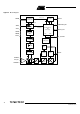
T5760/T5761 Pin Configuration Figure 3. Pinning SO20 SENS 1 20 DATA IC_ACTIVE 2 19 POLLING/_ON CDEM 3 18 DGND AVCC 4 17 DATA_CLK 16 TEST 4 15 DVCC TEST 1 5 T5760/ T5761 AGND 6 n.c. 7 14 XTAL LNAREF 8 13 n.c. LNA_IN 9 12 TEST 3 LNAGND 10 11 TEST 2 Pin Description Pin Symbol 1 SENS 2 IC_ACTIVE 3 CDEM Lower cut-off frequency data filter 4 AVCC Analog power supply 5 TEST 1 Test pin, during operation at GND 6 AGND Analog ground 7 n.c.
RF Front End The RF front end of the receiver is a low-IF heterodyne configuration that converts the input signal into a 950 kHz/1 MHz IF signal with an image rejection of typical 30 dB. According to Figure 3 the front end consists of an LNA (Low Noise Amplifier), LO (Local Oscillator), I/Q mixer, polyphase lowpass filter and an IF amplifier.
T5760/T5761 To determine fLO, the construction of the IF filter must be considered at this point. The nominal IF frequency is fIF = 950 kHz. To achieve a good accuracy of the filter corner frequencies, the filter is tuned by the crystal frequency fXTO. This means that there is a fixed relation between fIF and fLO. fIF = fLO/915 The relation is designed to achieve the nominal IF frequency of fIF = 950 kHz for the 868.3 MHz version. For the 915 MHz version an IF frequency of fIF = 1.0 MHz results.
Since different RF input networks may exhibit slightly different values for the LNA gain, the sensitivity values given in the electrical characteristics refer to a specific input matching. This matching is illustrated in Figure 33 and exhibits the best possible sensitivity and at the same time power matching at RF_IN. R Sens can be connected to V S or GND via a microcontroller. The receiver can be switched from full sensitivity to reduced sensitivity or vice versa at any time.
T5760/T5761 The T5760/T5761 is designed to operate with data coding where the DC level of the data signal is 50%. This is valid for Manchester and Bi-phase coding. If other modulation schemes are used, the DC level should always remain within the range of VDC_min = 33% and VDC_max = 66%. The sensitivity may be reduced by up to 2 dB in that condition. Each BR_Range is also defined by a minimum and a maximum edge-to-edge time (tee_sig). These limits are defined in the electrical characteristics.
Figure 7. Wide Band Receiving Frequency Response 0.0 -10.0 -20.0 -30.0 dP (dB) -40.0 -50.0 -60.0 -70.0 -80.0 -90.0 -100.0 -12.0 -9.0 -6.0 -3.0 0.0 3.0 6.0 9.0 12.0 df (MHz) Polling Circuit and Control Logic The receiver is designed to consume less than 1 mA while being sensitive to signals from a corresponding transmitter. This is achieved via the polling circuit. This circuit enables the signal path periodically for a short time.
T5760/T5761 • Application USA (fXTO = 7.14063 MHz, TClk = 1.961 µs) • Application Europe (fXTO = 6.77617 MHz, TClk = 2.066 µs) • Other applications The electrical characteristic is given as a function of TClk. The clock cycle of some function blocks depends on the selected baud-rate range (BR_Range) which is defined in the OPMODE register.
Figure 8. Polling Mode Flow Chart Sleep mode: All circuits for signal processing are disabled. Only XTO and Polling logic is enabled. Output level on Pin IC_ACTIVE => low IS = ISoff TSleep = Sleep x XSleep x 1024 x TClk Sleep: 5-bit word defined by Sleep0 to Sleep4 in OPMODE register Extension factor defined by XSleepStd according to Table 9 Basic clock cycle defined by fXTO and Pin MODE XSleep: TClk: Start-up mode: The signal processing circuits are enabled.
T5760/T5761 Bit-check Mode In bit-check mode the incoming data stream is examined to distinguish between a valid signal from a corresponding transmitter and signals due to noise. This is done by subsequent time frame checks where the distances between 2 signal edges are continuously compared to a programmable time window. The maximum count of this edge-to-edge tests before the receiver switches to receiving mode is also programmable.
Figure 14, Figure 15 and Figure 16 illustrate the bit check for the bit-check limits Lim_min = 14 and Lim_max = 24. When the IC is enabled, the signal processing circuits are enabled during TStartup. The output of the ASK/FSK demodulator (Dem_out) is undefined during that period. When the bit check becomes active, the bit-check counter is clocked with the cycle TXClk.
T5760/T5761 Duration of the Bit Check If no transmitter signal is present during the bit check, the output of the ASK/FSK demodulator delivers random signals. The bit check is a statistical process and TBit-check varies for each check. Therefore, an average value for TBit-check is given in the electrical characteristics. TBit-check depends on the selected baud-rate range and on TClk. A higher baud-rate range causes a lower value for TBit-check resulting in a lower current consumption in polling mode.
Figure 15. Debouncing of the Demodulator Output Dem_out Data_out (DATA) t DATA_min tDATA_min tee t DATA_min t ee t ee Figure 16. Steady L State Limited DATA Output Pattern After Transmission IC_ACTIVE Bit check Dem_out Data_out (DATA) tDATA_min Start-up mode Bit-check mode tDATA_L_max Receiving mode After the end of a data transmission, the receiver remains active.
T5760/T5761 Figure 17. Timing Diagram of the OFF Command via Pin DATA IC_ACTIVE t1 t2 t3 t5 t4 t10 t7 Out1 (microcontroller) Data_out (DATA) X Serial bi-directional data line X Bit 1 ("1") (Start bit) OFF-command Receiving mode TSleep TStart-up Sleep mode Start-up mode Figure 18.
Figure 18 illustrates how to set the receiver back to polling mode via Pin POLLING/_ON. The Pin POLLING/_ON must be held to low for the time period ton2. After the positive edge on Pin POLLING/_ON and the delay ton3, the polling mode is active and the sleep time TSleep elapses. This command is faster than using Pin DATA at the cost of an additional connection to the microcontroller. Figure 19 illustrates how to set the receiver to receiving mode via the Pin POLLING/_ON.
T5760/T5761 Figure 20. Timing Diagram of the Data Clock Preburst Data Bit check ok T '1' '1' '1' '1' 2T '1' '0' '1' '1' '0' '1' '0' Dem_out Data_out (DATA) DATA_CLK Start bit tDelay tP_Data_Clk Receiving mode, data clock control logic active Bit-check mode Figure 21.
Figure 23. Output of the Data Clock After a Successful Bit Check Data Bit check ok '1' '1' '1' '1' '1' '0' '1' '1' '0' '1' '0' Dem_out Data_out (DATA) DATA_CLK Start bit Receiving mode, bit check active Receiving mode, data clock control logic active The delay of the data clock is calculated as follows: tDelay = tDelay1 + tDelay2 tDelay1 is the delay between the internal signals Data_Out and Data_In.
T5760/T5761 Digital Noise Suppression After a data transmission, digital noise appears on the data output (see Figure 26). Preventing that digital noise keeps the connected microcontroller busy. It can be suppressed in two different ways. Automatic Noise Suppression If the bit Noise_Disable (Table 9) in the OPMODE register is set to 1 (default), the receiver changes to bit-check mode at the end of a valid data stream. The digital noise is suppressed and the level at Pin DATA is High in that case.
Controlled Noise Suppression by the Microcontroller Figure 29. Controlled Noise Suppression Bit check ok Serial bi-directional data line OFF-command Preburst Data Bit check ok Digital Noise Preburst Data Digital Noise (DATA_CLK) POLLING/_ON Bit-check mode Start-up Bit-check mode mode Receiving mode Receiving mode Sleep mode If the bit Noise_Disable (see Table 9) in the OPMODE register is set to 0, digital noise appears at the end of a valid data stream.
T5760/T5761 Table 3. Effect of the Configuration Words within the Registers Bit 1 Bit 2 Bit 3 Bit 4 Bit 5 Bit 6 Bit 7 Bit 8 Bit 9 Bit 10 Bit 11 Bit 12 Bit 13 Bit 14 – – – – – Bit 15 OFF command 1 – – – – – – – BR_Range 0 – – OPMODE register Modulation NBit-check 1 Baud1 Default values of Bit 3...
Table 6. Effect of the Configuration Bit Modulation Modulation Selected Modulation ASK/_FSK – 0 FSK (default) 1 ASK Table 7. Effect of the Configuration Word Sleep Sleep Start Value for Sleep Counter (TSleep = Sleep × Xsleep × 1024 × TClk) Sleep4 Sleep3 Sleep2 Sleep1 Sleep0 0 0 0 0 0 0 (Receiver is continuously polling until a valid signal occurs) 0 0 0 0 1 1 (TSleep » 2.1 ms for XSleep = 1 and fRF = 868.3 ms, » 2.0 ms for fRF = 915 MHz) 0 0 0 1 0 2 0 0 0 1 1 3 ... ..
T5760/T5761 Table 10. Effect of the Configuration Word Lim_min Lim_min (1) (Lim_min < 10 is not Applicable) Lower Limit Value for Bit Check Lim_min5 Lim_min4 Lim_min3 Lim_min2 Lim_min1 Lim_min0 (TLim_min = Lim_min × XLim × TClk) 0 0 1 0 1 0 10 0 0 1 0 1 1 11 0 0 1 1 0 0 12 .. .. .. .. .. .. 21 (default) (TLim_min = 347 µs for fRF = 868.3 MHz and BR_Range0 TLim_min = 329 µs for fRF = 915 MHz and BR_Range0) 0 1 0 1 0 1 .. .. .. .. .. ..
Conservation of the Register Information The T5760/T5761 implies an integrated power-on reset and brown-out detection circuitry to provide a mechanism to preserve the RAM register information. According to Figure 30, a power-on reset (POR) is generated if the supply voltage VS drops below the threshold voltage VThReset. The default parameters are programmed into the configuration registers in that condition. Once V S exceeds V ThReset the POR is canceled after the minimum reset period tRst.
T5760/T5761 Programming the Configuration Register Figure 31. Timing of the Register Programming IC_ACTIVE t1 t2 t3 Out1 (microcontroller) Data_out (DATA) X Serial bi-directional data line X t9 t8 t5 t4 t6 t7 Bit 1 ("0") (Start bit) Bit 2 ("1") (Registerselect) Bit 14 ("0") (Poll8) Bit 15 ("0") (Stop bit) TSleep TStart-up SleepStart-up mode mode Programming frame Receiving mode Figure 32. Data Interface V X = 5 V to 20 V T5760/ T5761 V S = 4.5 V to 5.
Bit 15 is followed by the equivalent time window t9. During this window, the equivalence acknowledge pulse t8 (E_Ack) occurs if the just programmed mode word is equivalent to the mode word that was already stored in that register. E_Ack should be used to verify that the mode word was correctly transferred to the register. The register must be programmed twice in that case. Programming of a register is possible both in sleep-mode and in active-mode of the receiver.
T5760/T5761 Figure 33. Application Circuit: fRF = 868.3 MHz without SAW Filter VS IC_ACTIVE C7 4.7u 10% R2 Sensitivity reduction 56k to 150k VX = 5 V to 20 V GND R3 >= 1.6k 1 SENS 2 IC_ACTIVE 3 CDEM C14 39n 5% 4 AVCC 5 TEST1 6 AGND C13 10n 10% 7 n.c. DATA POLLING/_ON DGND DATA_CLK TEST4 T5760/ T5761 C17 XTAL DATA POLLING/_ON DATA_CLK 15 Q1 C12 10n 10% 14 n.c. 13 12 TEST3 11 TEST2 8 LNAREF 9 LNA_IN 10 LNAGND RF_IN DVCC 20 19 18 17 16 6.77617 MHz C11 12p 2% np0 C16 1.5p ±0.
Absolute Maximum Ratings Parameters Symbol Min. Max. Unit Supply voltage VS 6 V Power dissipation Ptot 1000 mW Junction temperature Tj 150 °C Storage temperature Tstg -55 +125 °C Ambient temperature Tamb -40 +105 °C 10 dBm Maximum input level, input matched to 50 W Pin_max Thermal Resistance Parameters Junction ambient Symbol Value Unit RthJA 100 K/W Electrical Characteristics All parameters refer to GND, T amb = -40°C to +105°C, V S = 4.5 V to 5.5 V, f 0 = 868.
T5760/T5761 Electrical Characteristics (Continued) All parameters refer to GND, T amb = -40°C to +105°C, V S = 4.5 V to 5.5 V, f 0 = 868.3 MHz and f 0 = 915 MHz, unless otherwise specified. (For typical values: VS = 5 V, Tamb = 25°C) Parameter Test Conditions Time for bit check (see Figure 11) Bit-check time for a valid input signal fSig (see Figure 12) NBit-check = 0 NBit-check = 3 NBit-check = 6 NBit-check = 9 Symbol fRF = 868.3 MHz fRF = 915 MHz 6.77617 MHz Oscillator 7.
Electrical Characteristics (Continued) All parameters refer to GND, T amb = -40°C to +105°C, V S = 4.5 V to 5.5 V, f 0 = 868.3 MHz and f 0 = 915 MHz, unless otherwise specified. (For typical values: VS = 5 V, Tamb = 25°C) Parameter Test Conditions Symbol fRF = 868.3 MHz fRF = 915 MHz 6.77617 MHz Oscillator 7.14063 MHz Oscillator Min. Typ. Max. Min. 118.2 118.2 3355 2273 1731 1461 16397 11637 11637 11637 11637 Typ. Variable Oscillator Max. Min. 124.5 124.
T5760/T5761 Electrical Characteristics (continued) All parameters refer to GND, T amb = -40°C to +105°C, V S = 4.5 V to 5.5 V, f 0 = 868.3 MHz and f 0 = 915 MHz, unless otherwise specified. (For typical values: VS = 5 V, Tamb = 25°C) Parameters Test Conditions Symbol Current consumption Sleep mode (XTO and polling logic active) ISoff IC active (start-up-, bit-check-, receiving mode) Pin DATA = H FSK ASK ISon Min. Typ. Max. Unit 170 276 µA 7.8 7.4 9.9 9.
Electrical Characteristics (continued) All parameters refer to GND, T amb = -40°C to +105°C, V S = 4.5 V to 5.5 V, f 0 = 868.3 MHz and f 0 = 915 MHz, unless otherwise specified. (For typical values: VS = 5 V, Tamb = 25°C) Parameters Test Conditions Symbol Min. Sensitivity variation ASK for the full operating range compared to Tamb = 25°C, VS = 5 V fin = 868.
T5760/T5761 Electrical Characteristics (continued) All parameters refer to GND, T amb = -40°C to +105°C, V S = 4.5 V to 5.5 V, f 0 = 868.3 MHz and f 0 = 915 MHz, unless otherwise specified.
Electrical Characteristics (continued) All parameters refer to GND, T amb = -40°C to +105°C, V S = 4.5 V to 5.5 V, f 0 = 868.3 MHz and f 0 = 915 MHz, unless otherwise specified. (For typical values: VS = 5 V, Tamb = 25°C) Parameters Test Conditions Symbol Min. POLLING/_ON input - Low level input voltage - High level input voltage Receiving mode Polling mode VIl VIh 0.8´VS TEST 4 pin - High level input voltage Test input must always be set to High VIh 0.
Atmel Headquarters Atmel Operations Corporate Headquarters Memory 2325 Orchard Parkway San Jose, CA 95131 TEL 1(408) 441-0311 FAX 1(408) 487-2600 Europe Atmel Sarl Route des Arsenaux 41 Case Postale 80 CH-1705 Fribourg Switzerland TEL (41) 26-426-5555 FAX (41) 26-426-5500 Asia Room 1219 Chinachem Golden Plaza 77 Mody Road Tsimhatsui East Kowloon Hong Kong TEL (852) 2721-9778 FAX (852) 2722-1369 Japan 9F, Tonetsu Shinkawa Bldg.