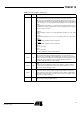
Features • 80C51 Core Architecture • 256 Bytes of On-chip RAM • 256 Bytes of On-chip ERAM • • • • • • • • • • • • • • • – 16-KB of On-chip Flash Memory – Data Retention: 10 Years at 85°C – Read/Write Cycle: 10K 2K Bytes of On-chip Flash for Bootloader 2K Bytes of On-chip EEPROM – Read/Write Cycle: 100k 14-sources 4-level Interrupts Three 16-bit Timers/Counters Full Duplex UART Compatible 80C51 Maximum Crystal Frequency 40 MHz – In X2 Mode, 20 MHz (CPU core, 40 MHz) Three or Four Ports: 16 or 20 Digital I
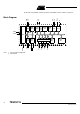
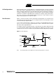
In X2 mode a maximum external clock rate of 20 MHz reaches a 300 ns cycle time. RAM 256x8 UART XTAL1 2 256x8 PCA T2 T2EX PCA ECI ERAM Timer2 IB-bus 10-bit ADC P4(2) P3 P2(2) Parallel I/O Ports & Ext. Bus Watch Dog Port 1 Port 2 Port 3 Port 4 P1(1) INT Ctrl INT1 T1 T0 RESET Timer 0 Timer 1 Notes: Flash Boot EEPROM 16kx8 loader 2kx8 2kx8 CPU INT0 XTAL2 C51 CORE Vss Vcc TxD RxD Block Diagram 1. 8 analog Inputs/8 Digital I/O 2.
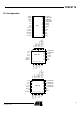
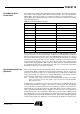
T89C5115 Pin Configuration VAREF VAGND VAVCC P4.1 P4.0 28 27 26 25 P2.1 P3.7 P3.6 P3.5/T1 P3.4/T0 P3.3/INT1 P3.2/INT0 1 2 3 4 5 6 7 8 9 10 11 12 P3.1/TxD 13 16 XTAL1 P3.0/RxD 14 15 XTAL2 RESET VSS VCC 4 3 2 1 28 27 26 P4.1 VAVCC VAGND VAREF P1.0/AN 0/T2 P1.1/AN1/T2EX P1.2/AN2/ECI SO28 24 23 22 21 20 19 18 17 P1.0/AN0/T2 P1.1/AN1/T2EX P1.2/AN2/ECI P1.3/AN3/CEX0 P1.4/AN4/CEX1 P1.5/AN5 P1.6/AN6 P1.7/AN7 P2.0 5 6 7 8 9 10 11 25 24 23 22 21 20 19 PLCC-28 P1.3/AN3/CEX0 P1.4/AN4/CEX1 P1.
Table 1. Pin Description Pin Name Type Description VSS GND Circuit ground VCC Supply Voltage VAREF Reference Voltage for ADC VAVCC Supply Voltage for ADC VAGND Reference Ground for ADC P1.0:7 I/O Port 1: Is an 8-bit bi-directional I/O port with internal pull-ups. Port 1 pins can be used for digital input/output or as analog inputs for the Analog Digital Converter (ADC).
T89C5115 Table 1. Pin Description (Continued) Pin Name Type P3.0:7 I/O Description Port 3: Is an 8-bit bi-directional I/O port with internal pull-ups. Port 3 pins that have 1’s written to them are pulled high by the internal pull-up transistors and can be used as inputs in this state. As inputs, Port 3 pins that are being pulled low externally will be a source of current (IIL, see section "Electrical Characteristic") because of the internal pull-ups.
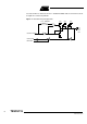
I/O Configurations Each Port SFR operates via type-D latches, as illustrated in Figure 1 for Ports 3 and 4. A CPU "write to latch" signal initiates transfer of internal bus data into the type-D latch. A CPU "read latch" signal transfers the latched Q output onto the internal bus. Similarly, a "read pin" signal transfers the logical level of the Port pin. Some Port data instructions activate the "read latch" signal while others activate the "read pin" signal.
T89C5115 Read-Modify-Write Instructions Some instructions read the latch data rather than the pin data. The latch based instructions read the data, modify the data and then rewrite the latch. These are called "ReadModify-Write" instructions. Below is a complete list of these special instructions (see Table ). When the destination operand is a Port or a Port bit, these instructions read the latch rather than the pin: Table 2.
associated nFET is switched off. This is traditional CMOS switch convention. Current strengths are 1/10 that of pFET #3 Figure 2. Internal Pull-Up Configurations 2 Osc. PERIODS VCC VCC VCC p1(1) p2 p3 P1.x P2.x P3.x P4.
T89C5115 SFR Mapping The Special Function Registers (SFRs) of the T89C5115 fall into the following categories: Table 3.
Table 5.
T89C5115 Table 8.
Table 11.
T89C5115 Clock The T89C5115 core needs only 6 clock periods per machine cycle. This feature, called ‘X2’, provides the following advantages: • Divides frequency crystals by 2 (cheaper crystals) while keeping the same CPU power. • Saves power consumption while keeping the same CPU power (oscillator power saving). • Saves power consumption by dividing dynamic operating frequency by 2 in operating and idle modes. • Increases CPU power by 2 while keeping the same crystal frequency.
Figure 3. Clock CPU Generation Diagram X2B Hardware byte PCON.0 On RESET IDL X2 CKCON.0 ÷2 XTAL1 CPU Core Clock 0 1 XTAL2 CPU CLOCK PD CPU Core Clock Symbol and ADC PCON.1 ÷2 1 FT0 Clock 0 ÷2 1 FT1 Clock 0 ÷2 1 FT2 Clock 0 ÷2 1 FUart Clock 0 ÷2 1 FPca Clock 0 ÷2 1 FWd Clock 0 PERIPH CLOCK X2 CKCON.0 Peripheral Clock Symbol 14 WDX2 PCAX2 SIX2 T2X2 T1X2 T0X2 CKCON.6 CKCON.5 CKCON.4 CKCON.3 CKCON.2 CKCON.
T89C5115 Figure 4. Mode Switching Waveforms XTAL1 XTAL2 X2 bit CPU clock STD Mode Note: X2 Mode STD Mode In order to prevent any incorrect operation while operating in the X2 mode, users must be aware that all peripherals using the clock frequency as a time reference (UART, timers...) will have their time reference divided by two. For example a free running timer generating an interrupt every 20 ms will then generate an interrupt every 10 ms. A UART with a 4800 baud rate will have a 9600 baud rate.
Register Table 12. CKCON Register CKCON (S:8Fh) Clock Control Register 7 6 5 4 3 2 1 0 – WDX2 PCAX2 SIX2 T2X2 T1X2 T0X2 X2 Bit Number Bit Mnemonic Description Reserved The value read from this bit is indeterminate. Do not set this bit. 7 - 6 WDX2 5 PCAX2 Programmable Counter Array clock(1) Clear to select 6 clock periods per peripheral clock cycle. Set to select 12 clock periods per peripheral clock cycle.
T89C5115 Power Management Introduction Two power reduction modes are implemented in the T89C5115: the Idle mode and the Power-down mode. These modes are detailed in the following sections. In addition to these power reduction modes, the clocks of the core and peripherals can be dynamically divided by 2 using the X2 mode detailed in Section “Clock”. Reset A reset is required after applying power at turn-on.
Idle Mode Idle mode is a power reduction mode that reduces the power consumption. In this mode, program execution halts. Idle mode freezes the clock to the CPU at known states while the peripherals continue to be clocked. The CPU status before entering Idle mode is preserved, i.e., the program counter and program status word register retain their data for the duration of Idle mode. The contents of the SFRs and RAM are also retained. The status of the Port pins during Idle mode is detailed in Table 13.
T89C5115 Exiting Power-down Mode Note: If VDD was reduced during the Power-down mode, do not exit Power-down mode until VDD is restored to the normal operating level. There are two ways to exit the Power-down mode: 1. Generate an enabled external interrupt. – Notes: The T89C5115 provides capability to exit from Power-down using INT0#, INT1#. Hardware clears PD bit in PCON register which starts the oscillator and restores the clocks to the CPU and peripherals.
Registers PCON (S:87h) Table 14. PCON Register Power Configuration Register 7 6 5 4 3 2 1 0 – – – – GF1 GF0 PD IDL Bit Number 7-4 Bit Mnemonic Description – Reserved The value read from these bits is indeterminate. Do not set these bits. 3 GF1 General-purpose flag 1 One use is to indicate whether an interrupt occurred during normal operation or during Idle mode.
T89C5115 Data Memory The T89C5115 provides data memory access in two different spaces: The internal space mapped in three separate segments: • the lower 128 bytes RAM segment. • the upper 128 bytes RAM segment. • the expanded 256 bytes RAM segment (ERAM). A fourth internal segment is available but dedicated to Special Function Registers, SFRs, (addresses 80h to FFh) accessible by direct addressing mode. Figure 7 shows the internal data memory spaces organization. Figure 7.
Figure 8. Lower 128 bytes Internal RAM Organization 7Fh 30h 2Fh 20h 18h 10h 08h 00h Bit-Addressable Space (Bit Addresses 0-7Fh) 1Fh 17h 0Fh 4 Banks of 8 Registers R0-R7 07h Upper 128 Bytes RAM The upper 128 bytes of RAM are accessible from address 80h to FFh using only indirect addressing mode. Expanded RAM The on-chip 256 bytes of expanded RAM (ERAM) are accessible from address 0000h to 00FFh using indirect addressing mode through MOVX instructions. In this address range.
T89C5115 Dual Data Pointer Description The T89C5115 implements a second data pointer for speeding up code execution and reducing code size in case of intensive usage of external memory accesses. DPTR0 and DPTR1 are seen by the CPU as DPTR and are accessed using the SFR addresses 83h and 84h that are the DPH and DPL addresses. The DPS bit in AUXR1 register (see Figure 17) is used to select whether DPTR is the data pointer 0 or the data pointer 1 (see Figure 9). Figure 9.
Registers Table 16. PSW Register PSW (S:8Eh) Program Status Word Register 7 6 5 4 3 2 1 0 CY AC F0 RS1 RS0 OV F1 P Bit Number Bit Mnemonic Description 7 CY Carry Flag Carry out from bit 1 of ALU operands. 6 AC Auxiliary Carry Flag Carry out from bit 1 of addition operands. 5 F0 User Definable Flag 0 4-3 RS1:0 2 OV Overflow Flag Overflow set by arithmetic operations. 1 F1 User Definable Flag 1 0 P Parity Bit Set when ACC contains an odd number of 1’s.
T89C5115 Table 17. AUXR1 Register AUXR1 (S:A2h) Auxiliary Control Register 1 7 6 5 4 3 2 1 0 – – ENBOOT – GF3 0 – DPS Bit Number 7-6 5 4 Bit Mnemonic Description – ENBOOT – Reserved The value read from these bits is indeterminate. Do not set these bits. Enable Boot Flash Set this bit for map the boot flash between F800h -FFFFh Clear this bit for disable boot flash. Reserved The value read from this bit is indeterminate. Do not set this bit. 3 GF3 General-purpose Flag 3.
EEPROM Data Memory The 2-kbyte on-chip EEPROM memory block is located at addresses 0000h to 07FFh of the XRAM/ERAM memory space and is selected by setting control bits in the EECON register. A read in the EEPROM memory is done with a MOVX instruction. A physical write in the EEPROM memory is done in two steps: write data in the column latches and transfer of all data latches into an EEPROM memory row (programming). The number of data written on the page may vary from 1 up to 128 bytes (the page size).
T89C5115 Examples ;*F************************************************************************* ;* NAME: api_rd_eeprom_byte ;* DPTR contain address to read.
Registers Table 18. EECON Register EECON (S:0D2h) EEPROM Control Register 7 6 5 4 3 2 1 0 EEPL3 EEPL2 EEPL1 EEPL0 - - EEE EEBUSY Bit Number Bit Mnemonic 7-4 EEPL3-0 Programming Launch Command bits Write 5Xh followed by AXh to EEPL to launch the programming. 3 - Reserved The value read from this bit is indeterminate. Do not set this bit. 2 - Reserved The value read from this bit is indeterminate. Do not set this bit.
T89C5115 Program/Code Memory The T89C5115 implement 16-KB of on-chip program/code memory. The Flash memory increases EPROM and ROM functionality by in-circuit electrical erasure and programming. Thanks to the internal charge pump, the high voltage needed for programming or erasing Flash cells is generated on-chip using the standard VDD voltage. Thus, the Flash Memory can be programmed using only one voltage and allows InSystem Programming commonly known as ISP.
FM0 Memory Architecture The Flash memory is made up of 4 blocks (see Figure 11): 1. The memory array (user space) 16-KB. 2. The Extra Row. 3. The Hardware security bits. 4. The column latch registers. User Space This space is composed of a 16-KB Flash memory organized in 128 pages of 128 bytes. It contains the user’s application code. Extra Row (XROW) This row is a part of FM0 and has a size of 128 bytes. The extra row may contain information for boot loader usage.
T89C5115 Overview of FM0 Operations The CPU interfaces to the Flash memory through the FCON register and AUXR1 register. These registers are used to: • Map the memory spaces in the adressable space • Launch the programming of the memory spaces • Get the status of the flash memory (busy/not busy) Mapping of the Memory Space By default, the user space is accessed by MOVC instruction for read only. The column latches space is made accessible by setting the FPS bit in FCON register.
Interrupts that may occur during programming time must be disabled to avoid any spurious exit of the programming mode. Status of the Flash Memory The bit FBUSY in FCON register is used to indicate the status of programming. FBUSY is set when programming is in progress. Selecting FM1 The bit ENBOOT in AUXR1 register is used to map FM1 from F800h to FFFFh. Loading the Column Latches Any number of data from 1 byte to 128 bytes can be loaded in the column latches.
T89C5115 Figure 12. Column Latches Loading Procedure Column Latches Loading Save & Disable IT EA= 0 Column Latches Mapping FCON = 08h (FPS=1) Data Load DPTR= Address ACC= Data Exec: MOVX @DPTR, A Last Byte to load? Data memory Mapping FCON = 00h (FPS = 0) Restore IT Note: The last page address used when loading the column latch is the one used to select the page programming address.
Figure 13. Flash and Extra row Programming Procedure Flash Spaces Programming Column Latches Loading see Figure 12 Save & Disable IT EA= 0 Launch Programming FCON= 5xh FCON= Axh FBusy Cleared? Clear Mode FCON = 00h End Programming Restore IT Hardware Security Byte 34 The following procedure is used to program the Hardware Security Byte space and is summarized in Figure 14: • Set FPS and map Hardware byte (FCON = 0x0C) • Save and disable the interrupts. • Load DPTR at address 0000h.
T89C5115 Figure 14. Hardware Programming Procedure Flash Spaces Programming Save & Disable IT EA= 0 Save & Disable IT EA= 0 FCON = 0Ch Launch Programming FCON= 54h FCON= A4h Data Load DPTR= 00h ACC= Data Exec: MOVX @DPTR, A FBusy Cleared? End Loading Restore IT Clear Mode FCON = 00h End Programming RestoreIT Reading the Flash Spaces User The following procedure is used to read the User space: • Read one byte in Accumulator by executing MOVC A,@A+DPTR with A+DPTR=read@.
Figure 15. Reading Procedure Flash Spaces Reading Flash Spaces Mapping FCON= 00000xx0b Data Read DPTR= Address ACC= 0 Exec: MOVC A, @A+DPTR Clear Mode FCON = 00h Flash Protection from Parallel Programming The three lock bits in Hardware Security Byte (see "In-System Programming" section) are programmed according to Table 22 provide different level of protection for the onchip code and data located in FM0 and FM1. The only way to write this bits are the parallel mode. They are set by default to level 3.
T89C5115 Registers FCON Register FCON (S:D1h) Flash Control Register 7 6 5 4 3 2 1 0 FPL3 FPL2 FPL1 FPL0 FPS FMOD1 FMOD0 FBUSY Bit Number Bit Mnemonic Description 7-4 FPL3:0 3 FPS 2-1 FMOD1:0 0 FBUSY Programming Launch Command Bits Write 5Xh followed by AXh to launch the programming according to FMOD1:0. (see Table 21.) Flash Map Program Space Set to map the column latch space in the data memory space. Clear to re-map the data memory space. Flash Mode See Table 20 or Table 21.
In-System Programming (ISP) With the implementation of the User Space (FM0) and the Boot Space (FM1) in Flash technology the T89C5115 allows the system engineer the development of applications with a very high level of flexibility. This flexibility is based on the possibility to alter the customer program at any stages of a product’s life: • Before assembly the 1st personalization of the product by programming in the FM0 and if needed also a customized Boot loader in the FM1.
T89C5115 Boot Process Software Boot Process Example Many algorithms can be used for the software boot process. Before describing them, The description of the different flags and bytes is given below: Boot Loader Jump Bit (BLJB): - This bit indicates if on RESET the user wants to jump to this application at address @0000h on FM0 or execute the boot loader at address @F800h on FM1. - BLJB = 0 on parts delivered with bootloader programmed. - To read or modify this bit, the APIs are used.
Application Programming Interface Several Application Program Interface (API) calls are available for use by an application program to permit selective erasing and programming of Flash pages. All calls are made by functions. All APIs are describe in: "In-System Programing: Flash Library for T89C5115", available on the Atmel web site at www.atmel.com. Table 23.
T89C5115 Hardware Security Byte Table 25. Hardware Security byte 7 6 5 4 3 2 1 0 X2B BLJB - - - LB2 LB1 LB0 Bit Number Bit Mnemonic Description 7 X2B X2 Bit Set this bit to start in standard mode Clear this bit to start in X2 mode. 6 BLJB Boot Loader Jump Bit - 1: To start the user’s application on next RESET (@0000h) located in FM0, - 0: To start the boot loader(@F800h) located in FM1. 5-3 - 2-0 LB2:0 Reserved The value read from these bits are indeterminate.
Serial I/O Port The T89C5115 I/O serial port is compatible with the I/O serial port in the 80C52. It provides both synchronous and asynchronous communication modes. It operates as a Universal Asynchronous Receiver and Transmitter (UART) in three full-duplex modes (Modes 1, 2 and 3). Asynchronous transmission and reception can occur simultaneously and at different baud rates Serial I/O port includes the following enhancements: • Framing error detection • Automatic address recognition Figure 18.
T89C5115 valid stop bits cannot clear the FE bit. When the FE feature is enabled, RI rises on the stop bit instead of the last data bit (See Figure 20 and Figure 21). Figure 20. UART Timing in Mode 1 RXD D0 D1 D2 D3 D4 D5 D6 D7 Data byte Start bit Stop bit RI SMOD0=X FE SMOD0=1 Figure 21.
Given Address Each device has an individual address that is specified in the SADDR register; the SADEN register is a mask byte that contains don’t-care bits (defined by zeros) to form the device’s given address. The don’t-care bits provide the flexibility to address one or more slaves at a time. The following example illustrates how a given address is formed. To address a device by its individual address, the SADEN mask byte must be 1111 1111b.
T89C5115 For slaves A and B, bit 2 is a don’t care bit; for slave C, bit 2 is set. To communicate with all of the slaves, the master must send an address FFh. To communicate with slaves A and B, but not slave C, the master can send and address FBh. Registers Table 26.
Table 27. SADEN Register SADEN (S:B9h) Slave Address Mask Register 7 Bit Number 7-0 6 5 4 3 2 1 0 3 2 1 0 Bit Mnemonic Description – Mask Data for Slave Individual Address Reset Value = 0000 0000b Not bit addressable Table 28. SADDR Register SADDR (S:A9h) Slave Address Register 7 Bit Number 7-0 6 5 4 Bit Mnemonic Description – Slave Individual Address Reset Value = 0000 0000b Not bit addressable Table 29.
T89C5115 Table 30. PCON Register PCON (S:87h) Power Control Register 7 6 5 4 3 2 1 0 SMOD1 SMOD0 - POF GF1 GF0 PD IDL Bit Number Bit Mnemonic Description 7 SMOD1 Serial port Mode bit 1 Set to select double baud rate in mode 1, 2 or 3. 6 SMOD0 Serial port Mode bit 0 Clear to select SM0 bit in SCON register. Set to select FE bit in SCON register. 5 - Reserved The value read from this bit is indeterminate. Do not set this bit.
Timers/Counters The T89C5115 implements two general-purpose, 16-bit Timers/Counters. Such are identified as Timer 0 and Timer 1, and can be independently configured to operate in a variety of modes as a Timer or an event Counter. When operating as a Timer, the Timer/Counter runs for a programmed length of time, then issues an interrupt request. When operating as a Counter, the Timer/Counter counts negative transitions on an external pin.
T89C5115 Mode 0 (13-bit Timer) Mode 0 configures Timer 0 as an 13-bit Timer which is set up as an 8-bit Timer (TH0 register) with a modulo 32 prescaler implemented with the lower five bits of TL0 register (see Figure 22). The upper three bits of TL0 register are indeterminate and should be ignored. Prescaler overflow increments TH0 register. Figure 22.
Mode 2 (8-bit Timer with AutoReload) Mode 2 configures Timer 0 as an 8-bit Timer (TL0 register) that automatically reloads from TH0 register (see Figure 24). TL0 overflow sets TF0 flag in TCON register and reloads TL0 with the contents of TH0, which is preset by software. When the interrupt request is serviced, hardware clears TF0. The reload leaves TH0 unchanged. The next reload value may be changed at any time by writing it to TH0 register. Figure 24.
T89C5115 Timer 1 Timer 1 is identical to Timer 0 excepted for Mode 3 which is a hold-count mode. Following comments help to understand the differences: • Timer 1 functions as either a Timer or event Counter in three modes of operation. Figure 22 to Figure 24 show the logical configuration for modes 0, 1, and 2. Timer 1’s mode 3 is a hold-count mode. • Timer 1 is controlled by the four high-order bits of TMOD register (see Figure 32) and bits 2, 3, 6 and 7 of TCON register (see Figure 31).
Interrupt Each Timer handles one interrupt source that is the timer overflow flag TF0 or TF1. This flag is set every time an overflow occurs. Flags are cleared when vectoring to the Timer interrupt routine. Interrupts are enabled by setting ETx bit in IEN0 register. This assumes interrupts are globally enabled by setting EA bit in IEN0 register. Figure 26. Timer Interrupt System Timer 0 Interrupt Request TF0 TCON.5 ET0 IEN0.1 Timer 1 Interrupt Request TF1 TCON.7 ET1 IEN0.
T89C5115 Registers Table 31. TCON Register TCON (S:88h) Timer/Counter Control Register 7 6 5 4 3 2 1 0 TF1 TR1 TF0 TR0 IE1 IT1 IE0 IT0 Bit Number Bit Mnemonic Description 7 TF1 Timer 1 Overflow Flag Cleared by hardware when processor vectors to interrupt routine. Set by hardware on Timer/Counter overflow, when Timer 1 register overflows. 6 TR1 Timer 1 Run Control Bit Clear to turn off Timer/Counter 1. Set to turn on Timer/Counter 1.
Table 32. TMOD Register TMOD (S:89h) Timer/Counter Mode Control Register 7 6 5 4 3 2 1 0 GATE1 C/T1# M11 M01 GATE0 C/T0# M10 M00 Bit Number Bit Mnemonic Description 7 GATE1 Timer 1 Gating Control Bit Clear to enable Timer 1 whenever TR1 bit is set. Set to enable Timer 1 only while INT1# pin is high and TR1 bit is set. 6 C/T1# Timer 1 Counter/Timer Select Bit Clear for Timer operation: Timer 1 counts the divided-down system clock.
T89C5115 Table 33. TH0 Register TH0 (S:8Ch) Timer 0 High Byte Register 7 Bit Number 6 5 4 3 2 1 0 3 2 1 0 3 2 1 0 Bit Mnemonic Description 7:0 High Byte of Timer 0. Reset Value = 0000 0000b Table 34. TL0 Register TL0 (S:8Ah) Timer 0 Low Byte Register 7 Bit Number 6 5 4 Bit Mnemonic Description 7:0 Low Byte of Timer 0. Reset Value = 0000 0000b Table 35. TH1 Register TH1 (S:8Dh) Timer 1 High Byte Register 7 Bit Number 7:0 6 5 4 Bit Mnemonic Description High Byte of Timer 1.
Table 36. TL1 Register TL1 (S:8Bh) Timer 1 Low Byte Register 7 Bit Number 7:0 6 5 4 3 2 1 0 Bit Mnemonic Description Low Byte of Timer 1.
T89C5115 Timer 2 The T89C5115 Timer 2 is compatible with Timer 2 in the 80C52. It is a 16-bit timer/counter: the count is maintained by two eight-bit timer registers, TH2 and TL2 that are cascade- connected. It is controlled by T2CON register (See Table ) and T2MOD register (See Table 39). Timer 2 operation is similar to Timer 0 and Timer 1. C/T2 selects F T2 clock/6 (timer operation) or external pin T2 (counter operation) as timer clock. Setting TR2 allows TL2 to be incremented by the selected input.
Programmable ClockOutput In clock-out mode, Timer 2 operates as a 50%-duty-cycle, programmable clock generator (See Figure 28). The input clock increments TL2 at frequency FOSC /2. The timer repeatedly counts to overflow from a loaded value. At overflow, the contents of RCAP2H and RCAP2L registers are loaded into TH2 and TL2. In this mode, Timer 2 overflows do not generate interrupts.
T89C5115 Registers Table 37. T2CON Register T2CON (S:C8h) Timer 2 Control Register 7 6 5 4 3 2 1 0 TF2 EXF2 RCLK TCLK EXEN2 TR2 C/T2# CP/RL2# Bit Number 7 Bit Mnemonic Description TF2 Timer 2 overflow Flag TF2 is not set if RCLK=1 or TCLK = 1. Must be cleared by software. Set by hardware on Timer 2 overflow. 6 EXF2 Timer 2 External Flag Set when a capture or a reload is caused by a negative transition on T2EX pin if EXEN2=1.
Table 38. T2MOD Register T2MOD (S:C9h) Timer 2 Mode Control Register 7 6 5 4 3 2 1 0 - - - - - - T2OE DCEN Bit Number Bit Mnemonic Description 7 - Reserved The value read from this bit is indeterminate. Do not set this bit. 6 - Reserved The value read from this bit is indeterminate. Do not set this bit. 5 - Reserved The value read from this bit is indeterminate. Do not set this bit. 4 - Reserved The value read from this bit is indeterminate. Do not set this bit.
T89C5115 Table 40. TL2 Register TL2 (S:CCh) Timer 2 Low Byte Register 7 6 5 4 3 2 1 0 - - - - - - - - Bit Number Bit Mnemonic Description 7-0 Low Byte of Timer 2. Reset Value = 0000 0000b Not bit addressable Table 41. RCAP2H Register RCAP2H (S:CBh) Timer 2 Reload/Capture High Byte Register 7 6 5 4 3 2 1 0 - - - - - - - - Bit Number Bit Mnemonic Description 7-0 High Byte of Timer 2 Reload/Capture. Reset Value = 0000 0000b Not bit addressable Table 42.
WatchDog Timer T89C5115 contains a powerful programmable hardware WatchDog Timer (WDT) that automatically resets the chip if it software fails to reset the WDT before the selected time interval has elapsed. It permits large Time-Out ranking from 16ms to 2s @Fosc = 12 MHz in X1 mode. This WDT consists of a 14-bit counter plus a 7-bit programmable counter, a WatchDog Timer reset register (WDTRST) and a WatchDog Timer programming (WDTPRG) register. When exiting reset, the WDT is -by default- disable.
T89C5115 WatchDog Programming The three lower bits (S0, S1, S2) located into WDTPRG register permit to program the WDT duration. Table 43.
WatchDog Timer during Power-down Mode and Idle In Power-down mode the oscillator stops, which means the WDT also stops. While in Power-down mode, the user does not need to service the WDT. There are 2 methods of exiting Power-down mode: by a hardware reset or via a level activated external interrupt which is enabled prior to entering Power-down mode. When Power-down is exited with hardware reset, the WatchDog is disabled. Exiting Power-down with an interrupt is significantly different.
T89C5115 Table 46. WDTRST Register WDTRST (S:A6h Write only) WatchDog Timer Enable Register 7 6 5 4 3 2 1 0 - - - - - - - - Bit Number 7 Bit Mnemonic Description - WatchDog Control Value Reset Value = 1111 1111b Note: The WDRST register is used to reset/enable the WDT by writing 1EH then E1H in sequence without instruction between these two sequences.
Programmable Counter Array (PCA) The PCA provides more timing capabilities with less CPU intervention than the standard timer/counters. Its advantages include reduced software overhead and improved accuracy. The PCA consists of a dedicated timer/counter which serves as the time base for an array of five compare/capture modules.
T89C5115 Figure 30. PCA Timer/Counter To PCA modules FPca/6 overflow FPca/2 CH T0 OVF It CL 16 bit up/down counter P1.2 CIDL WDTE CF CR CPS1 CPS0 ECF CMOD 0xD9 Idle CCF1 CCF0 CCON 0xD8 The CMOD register includes three additional bits associated with the PCA. • The CIDL bit which allows the PCA to stop during idle mode. • The WDTE bit which enables or disables the WatchDog function on module 4.
PCA Modules Each one of the five compare/capture modules has six possible functions. It can perform: • 16-bit Capture, positive-edge triggered • 16-bit Capture, negative-edge triggered • 16-bit Capture, both positive and negative-edge triggered • 16-bit Software Timer • 16-bit High Speed Output • 8-bit Pulse Width Modulator. Each module in the PCA has a special function register associated with it (CCAPM0 for module 0 ...).
T89C5115 PCA Interrupt Figure 31. PCA Interrupt System CF CCF1 CCF0 CR CCON 0xD8 PCA Timer/Counter Module 0 Module 1 To Interrupt ECF CMOD.0 ECCFn CCAPMn.0 PCA Capture Mode EC EA IEN0.6 IEN0.7 To use one of the PCA modules in capture mode either one or both of the CCAPM bits CAPN and CAPP for that module must be set. The external CEX input for the module (on port 1) is sampled for a transition.
16-bit Software Timer Mode The PCA modules can be used as software timers by setting both the ECOM and MAT bits in the modules CCAPMn register. The PCA timer will be compared to the module’s capture registers and when a match occurs an interrupt will occur if the CCFn (CCON SFR) and the ECCFn (CCAPMn SFR) bits for the module are both set. Figure 33.
T89C5115 High Speed Output Mode In this mode the CEX output (on port 1) associated with the PCA module will toggle each time a match occurs between the PCA counter and the module’s capture registers. To activate this mode the TOG, MAT, and ECOM bits in the module’s CCAPMn SFR must be set. Figure 34.
Figure 35. PCA PWM Mode CCAPnH CL rolls over from FFh TO 00h loads CCAPnH contents into CCAPnL CCAPnL “0” CL < CCAPnL CL (8 bits) 8-Bit Comparator CEX CL >= CCAPnL “1” 72 ECOMn PWMn CCAPMn.6 CCAPMn.
T89C5115 PCA Registers Table 47. CMOD Register CMOD (S:D9h) PCA Counter Mode Register 7 6 5 4 3 2 1 0 CIDL WDTE - - - CPS1 CPS0 ECF Bit Number Bit Mnemonic Description PCA Counter Idle Control bit Clear to let the PCA run during Idle mode. Set to stop the PCA when Idle mode is invoked. 7 CIDL 6 WDTE 5 - Reserved The value read from this bit is indeterminate. Do not set this bit. 4 - Reserved The value read from this bit is indeterminate. Do not set this bit.
Table 48. CCON Register CCON (S:D8h) PCA Counter Control Register 7 6 5 4 3 2 1 0 CF CR - - - - CCF1 CCF0 Bit Number Bit Mnemonic Description 7 CF PCA Timer/Counter Overflow flag Set by hardware when the PCA Timer/Counter rolls over. This generates a PCA interrupt request if the ECF bit in CMOD register is set. Must be cleared by software. 6 CR PCA Timer/Counter Run Control bit Clear to turn the PCA Timer/Counter off. Set to turn the PCA Timer/Counter on.
T89C5115 Table 49. CCAPnH Registers CCAP0H (S:FAh) CCAP1H (S:FBh) PCA High Byte Compare/Capture Module n Register (n=0..1) 7 6 5 4 3 2 1 0 CCAPnH 7 CCAPnH 6 CCAPnH 5 CCAPnH 4 CCAPnH 3 CCAPnH 2 CCAPnH 1 CCAPnH 0 Bit Number 7:0 Bit Mnemonic Description CCAPnH 7:0 High byte of EWC-PCA comparison or capture values Reset Value = 0000 0000b Table 50. CCAPnL Registers CCAP0L (S:EAh) CCAP1L (S:EBh) PCA Low Byte Compare/Capture Module n Register (n=0..
Table 51. CCAPMn Registers CCAPM0 (S:DAh) CCAPM1 (S:DBh) PCA Compare/Capture Module n Mode registers (n=0..1) 7 6 5 4 3 2 1 0 - ECOMn CAPPn CAPNn MATn TOGn PWMn ECCFn Bit Number 7 Bit Mnemonic Description - Reserved The Value read from this bit is indeterminate. Do not set this bit. 6 ECOMn Enable Compare Mode Module x bit Clear to disable the Compare function. Set to enable the Compare function.
T89C5115 Table 52. CH Register CH (S:F9h) PCA Counter Register High Value 7 6 5 4 3 2 1 0 CH 7 CH 6 CH 5 CH 4 CH 3 CH 2 CH 1 CH 0 Bit Number 7:0 Bit Mnemonic Description CH 7:0 High byte of Timer/Counter Reset Value = 0000 00000b Table 53.
Analog-to-Digital Converter (ADC) This section describes the on-chip 10-bit analog-to-digital converter of the T89C5115. Eight ADC channels are available for sampling of the external sources AN0 to AN7. An analog multiplexer allows the single ADC converter to select one from the 8 ADC channels as ADC input voltage (ADCIN). ADCIN is converted by the 10 bit-cascaded potentiometric ADC. Two kind of conversion are available: - Standard conversion (8 bits). - Precision conversion (10 bits).
T89C5115 Figure 36. ADC Description ADCON.5 ADCON.3 ADEN ADSST ADC Interrupt Request ADCON.4 ADEOC ADC CLOCK CONTROL EADC AN0/P1.0 000 AN1/P1.1 001 AN2/P1.2 010 AN3/P1.3 011 AN4/P1.4 100 AN5/P1.5 101 AN6/P1.6 110 AN7/P1.7 IEN1.1 ADCIN 8 ADDH 2 ADDL + SAR - AVSS Sample and Hold 111 10 R/2R DAC SCH2 SCH1 SCH0 ADCON.2 ADCON.1 ADCON.0 VAREF VAGND Figure 37 shows the timing diagram of a complete conversion.
Table 54. Selected Analog Input Voltage Conversion SCH2 SCH1 SCH0 Selected Analog input 0 0 0 AN0 0 0 1 AN1 0 1 0 AN2 0 1 1 AN3 1 0 0 AN4 1 0 1 AN5 1 1 0 AN6 1 1 1 AN7 When the ADCIN is equals to VAREF the ADC converts the signal to 3FFh (full scale). If the input voltage equals VAGND, the ADC converts it to 000h. Input voltage between VAREF and VAGND are a straight-line linear conversion.
T89C5115 IT ADC Management An interrupt end-of-conversion will occurs when the bit ADEOC is activated and the bit EADC is set. For re-arming the interrupt the bit ADEOC must be cleared by software. Figure 39. ADC interrupt structure ADCI ADEOC ADCON.2 EADC IEN1.1 Routine Examples 1. Configure P1.2 and P1.3 in ADC channels // configure channel P1.2 and P1.3 for ADC ADCF = 0Ch // Enable the ADC ADCON = 20h 2.
Registers Table 55. ADCF Register ADCF (S:F6h) ADC Configuration 7 6 5 4 3 2 1 0 CH 7 CH 6 CH 5 CH 4 CH 3 CH 2 CH 1 CH 0 Bit Number 7-0 Bit Mnemonic Description CH 0:7 Channel Configuration Set to use P1.x as ADC input. Clear to use P1.x as standart I/O port. Reset Value = 0000 0000b Table 56.
T89C5115 Table 57. ADCLK Register ADCLK (S:F2h) ADC Clock Prescaler 7 6 5 4 3 2 1 0 - - - PRS 4 PRS 3 PRS 2 PRS 1 PRS 0 Bit Number Bit Mnemonic Description 7-5 - 4-0 PRS4:0 Reserved The value read from these bits are indeterminate. Do not set these bits. Clock Prescaler fADC = fcpu clock/ (4 (or 2 in X2 mode)* (PRS +1)) Reset Value = XXX0 0000b Table 58.
Interrupt System Introduction The T89C5115 has a total of 8 interrupt vectors: two external interrupts (INT0 and INT1), three timer interrupts (timers 0, 1 and 2), a serial port interrupt, a PCAand an ADC. These interrupts are shown below. Figure 40. Interrupt Control System INT0# 00 01 10 11 External Interrupt 0 Highest Priority Interrupts EX0 00 01 10 11 IEN0.0 Timer 0 ET0 INT1# External Interrupt 1 00 01 10 11 IEN0.1 EX1 00 01 10 11 IEN0.2 Timer 1 ET1 CEX0:1 PCA 00 01 10 11 IEN0.
T89C5115 Table 60. Priority Level Bit Values IPH.x IPL.x Interrupt Level Priority 0 0 0 (Lowest) 0 1 1 1 0 2 1 1 3 (Highest) A low-priority interrupt can be interrupted by a high priority interrupt but not by another low-priority interrupt. A high-priority interrupt cannot be interrupted by any other interrupt source. If two interrupt requests of different priority levels are received simultaneously, the request of the higher priority level is serviced.
Registers Table 62. IEN0 Register IEN0 (S:A8h) Interrupt Enable Register 7 6 5 4 3 2 1 0 EA EC ET2 ES ET1 EX1 ET0 EX0 Bit Number Bit Mnemonic Description 7 EA Enable All interrupt bit Clear to disable all interrupts. Set to enable all interrupts. If EA=1, each interrupt source is individually enabled or disabled by setting or clearing its interrupt enable bit. 6 EC PCA Interrupt Enable Clear to disable the PCA interrupt. Set to enable the PCA interrupt.
T89C5115 Table 63. IEN1 Register IEN1 (S:E8h) Interrupt Enable Register 7 6 5 4 3 2 1 0 - - - - - - EADC - Bit Number Bit Mnemonic Description 7 - Reserved The value read from this bit is indeterminate. Do not set this bit. 6 - Reserved The value read from this bit is indeterminate. Do not set this bit. 5 - Reserved The value read from this bit is indeterminate. Do not set this bit. 4 - Reserved The value read from this bit is indeterminate. Do not set this bit.
Table 64. IPL0 Register IPL0 (S:B8h) Interrupt Enable Register 7 6 5 4 3 2 1 0 - PPC PT2 PS PT1 PX1 PT0 PX0 Bit Number Bit Mnemonic Description Reserved The value read from this bit is indeterminate. Do not set this bit. 7 - 6 PPC PCA Interrupt Priority bit Refer to PPCH for priority level. 5 PT2 Timer 2 overflow interrupt Priority bit Refer to PT2H for priority level. 4 PS Serial port Priority bit Refer to PSH for priority level.
T89C5115 Table 65. IPL1 Register IPL1 (S:F8h) Interrupt Priority Low Register 1 7 6 5 4 3 2 1 0 - - - - - - PADCL - Bit Number Bit Mnemonic Description 7 - Reserved The value read from this bit is indeterminate. Do not set this bit. 6 - Reserved The value read from this bit is indeterminate. Do not set this bit. 5 - Reserved The value read from this bit is indeterminate. Do not set this bit. 4 - Reserved The value read from this bit is indeterminate. Do not set this bit.
Table 66. IPL0 Register IPH0 (B7h) Interrupt High Priority Register 7 6 5 4 3 2 1 0 - PPCH PT2H PSH PT1H PX1H PT0H PX0H Bit Number 7 6 5 4 3 2 1 0 Bit Mnemonic Description - Reserved The value read from this bit is indeterminate. Do not set this bit.
T89C5115 Table 67. IPH1 Register IPH1 (S:F7h) Interrupt high priority Register 1 7 6 5 4 3 2 1 0 - - - - - - PADCH - Bit Number Bit Mnemonic Description 7 - Reserved The value read from this bit is indeterminate. Do not set this bit. 6 - Reserved The value read from this bit is indeterminate. Do not set this bit. 5 - Reserved The value read from this bit is indeterminate. Do not set this bit. 4 - Reserved The value read from this bit is indeterminate. Do not set this bit.
Electrical Characteristics Absolute Maximum Ratings Note: Ambiant Temperature Under Bias: I = industrial ....................................................... -40°C to 85°C Storage Temperature ................................... -65°C to + 150°C Voltage on VCC from VSS ......................................-0.5V to + 6V Voltage on Any Pin from V SS ....................-0.5V to V CC + 0.2 V Power Dissipation .............................................................
T89C5115 5. Under steady state (non-transient) conditions, IOL must be externally limited as follows: Maximum IOL per port pin: 10 mA Maximum IOL per 8-bit port: Ports 1, 2 and 3: 15 mA Maximum total IOL for all output pins: 71 mA If IOL exceeds the test condition, VOL may exceed the related specification. Pins are not guaranteed to sink current greater than the listed test conditions. Figure 41.
Figure 44. Clock Signal Waveform for ICC Tests in Active and Idle Modes VCC-0.5V 0.45V TCLCH TCHCL TCLCH = TCHCL = 5ns. DC Parameters for A/D Converter Table 69. DC Parameters for AD Converter in Precision conversion Symbol Parameter Min Typ(1) Unit Vref + 0.6 V 24 kΩ 3.00 V Analog input voltage Rref Resistance between Vref and Vss Vref Reference voltage Cai Analog input Capacitance 60 INL Integral non linearity 1 2 lsb DNL Differential non linearity 0.
T89C5115 AC Parameters Explanation of the AC Symbols Each timing symbol has 5 characters. The first character is always a “T” (stands for time). The other characters, depending on their positions, stand for the name of a signal or the logical status of that signal. The following is a list of all the characters and what they stand for. Example: TAVLL = Time for Address Valid to ALE Low. TLLPL = Time for ALE Low to PSEN Low. TA = -40°C to +85°C; VSS = 0V; V CC = 5V ± 10%; F = 0 to 40 MHz.
Table 72.
T89C5115 Float Waveforms FLOAT VOH - 0.1 V VLOAD + 0.1 V VLOAD VLOAD - 0.1 V VOL + 0.1 V For timing purposes as port pin is no longer floating when a 100 mV change from load voltage occurs and begins to float when a 100 mV change from the loaded VOH/V OL level occurs. IOL/IOH ≥ ± 20 mA. Flash Memory Table 74. Memory AC Timing VDD = 5V ± 10% , TA = -40 to +85°C Symbol Parameter Min TBHBL Flash Internal Busy (Programming) Time Typ 10 Max Unit ms Figure 45.
Ordering Information Table 75.
T89C5115 Package Drawing PLCC28 99 4128A–8051–04/02
Package Drawing SOIC28 100 T89C5115 4128A–8051–04/02
T89C5115 Package Drawing VQFP32 101 4128A–8051–04/02
T89C5115 Table of Contents Features ................................................................................................. 1 Description ............................................................................................ 1 Block Diagram ....................................................................................... 2 Pin Configuration .................................................................................. 3 I/O Configurations............................................
In-System Programming (ISP) ........................................................... 38 Flash Programming and Erasure ........................................................................ Boot Process ...................................................................................................... Application Programming Interface..................................................................... XROW Bytes.........................................................................................
T89C5115 Voltage Conversion ............................................................................................ 80 Clock Selection ................................................................................................... 80 ADC Standby Mode ............................................................................................ 80 IT ADC Management ...........................................................................................81 Routine Examples............................
Atmel Headquarters Atmel Operations Corporate Headquarters Memory 2325 Orchard Parkway San Jose, CA 95131 TEL 1(408) 441-0311 FAX 1(408) 487-2600 Europe Atmel Sarl Route des Arsenaux 41 Case Postale 80 CH-1705 Fribourg Switzerland TEL (41) 26-426-5555 FAX (41) 26-426-5500 Asia Room 1219 Chinachem Golden Plaza 77 Mody Road Tsimhatsui East Kowloon Hong Kong TEL (852) 2721-9778 FAX (852) 2722-1369 Japan 9F, Tonetsu Shinkawa Bldg.