. Features • 80C51 core architecture: – 256 bytes of on-chip RAM – 1 Kbytes of on-chip ERAM – 32 Kbytes of on-chip Flash memory Data Retention: 10 years at 85°C Read/Write cycle: 10k – 2 Kbytes of on-chip Flash for Bootloader – 2 Kbytes of on-chip EEPROM Read/Write cycle: 100k – 14-sources 4-level interrupts – Three 16-bit timers/counters – Full duplex UART compatible 80C51 – Maximum crystal frequency 40 MHz.
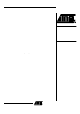
The added features of the T89C51AC2 make it more powerful for applications that need A/D conversion, pulse width modulation, high speed I/O and counting capabilities such as industrial control, consumer goods, alarms, motor control, etc. While remaining fully compatible with the 80C52 it offers a superset of this standard microcontroller. In X2 mode a maximum external clock rate of 20 MHz reaches a 300 ns cycle time. T2 T2EX PCA ECI Vss Vcc TxD RxD 3.
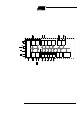
T89C51AC2 6 5 4 3 2 1 44 43 42 41 40 P1.3 / AN3 / CEX0 P1.2 / AN2 / ECI P1.1 / AN1 / T2EX P1.0 / AN 0 / T2 VAREF VAGND RESET VSS VCC XTAL1 XTAL2 4. Pin Configuration 7 8 9 10 11 12 13 14 15 16 17 39 38 37 36 35 34 33 32 31 30 29 PLCC44 ALE PSEN P0.7 / AD7 P0.6 / AD6 P0.5 / AD5 P0.4 / AD4 P0.3 / AD3 P0.2 / AD2 P0.1 / AD1 P0.0 / AD0 P2.0 / A8 P4.0 P4.1 P2.7 / A15 P2.6 / A14 P2.5 / A13 P2.4 / A12 P2.3 / A11 P2.2 / A10 P2.1 / A9 P1.3 / AN3 / CEX0 P1.2 / AN2 / ECI P1.1 / AN1 / T2EX P1.
Table 1. Pin Description Pin Name Type VSS GND VCC Description Circuit ground. Supply Voltage. VAREF Reference Voltage for ADC VAGND Reference Ground for ADC P0.0:7 I/O Port 0: Is an 8-bit open drain bi-directional I/O port. Port 0 pins that have 1’s written to them float, and in this state can be used as high-impedance inputs. Port 0 is also the multiplexed low-order address and data bus during accesses to external Program and Data Memory.
T89C51AC2 Pin Name P2.0:7 Type Description I/O Port 2: Is an 8-bit bi-directional I/O port with internal pull-ups. Port 2 pins that have 1’s written to them are pulled high by the internal pull-ups and can be used as inputs in this state. As inputs, Port 2 pins that are being pulled low externally will be a source of current (IIL, see section "Electrical Characteristic") because of the internal pull-ups.
Pin Name Type RESET I/O Reset: A high level on this pin during two machine cycles while the oscillator is running resets the device. An internal pulldown resistor to VSS permits power-on reset using only an external capacitor to VCC. ALE O ALE: An Address Latch Enable output for latching the low byte of the address during accesses to the external memory. The ALE is activated every 1/6 oscillator periods (1/3 in X2 mode) except during an external data memory access.
T89C51AC2 Figure 1. Port 1, Port 3 and Port 4 Structure VCC ALTERNATE OUTPUT FUNCTION READ LATCH INTERNAL BUS WRITE TO LATCH 4.3 Port 0 and Port2 P1.x P3.x P4.x D P1.X Q P3.X P4.X LATCH CL READ PIN Note: INTERNAL PULL-UP (1) ALTERNATE INPUT FUNCTION The internal pull-up can be disabled on P1 when analog function is selected. Ports 0 and 2 are used for general-purpose I/O or as the external address/data bus. Port 0, shown in Figure 3, differs from the other Ports in not having internal pull-ups.
Figure 3. Port 2 Structure ADDRESS HIGH/ CONTROL VDD INTERNAL PULL-UP (2) READ LATCH P2.x (1) 1 INTERNAL BUS WRITE TO LATCH D P2.X LATCH 0 Q READ PIN Notes: 1. Port 2 is precluded from use as general purpose I/O Ports when as address/data bus drivers. 2. Port 2 internal strong pull-ups FET (P1 in FiGURE) assist the logic-one output for memory bus cycle.
T89C51AC2 It is not obvious the last three instructions in this list are Read-Modify-Write instructions. These instructions read the port (all 8 bits), modify the specifically addressed bit and write the new byte back to the latch. These Read-Modify-Write instructions are directed to the latch rather than the pin in order to avoid possible misinterpretation of voltage (and therefore, logic) levels at the pin.
5. SFR Mapping The Special Function Registers (SFRs) of the T89C51AC2 fall into the following categories: Table 3. C51 Core SFRs Mnemonic Add Name ACC E0h Accumulator B F0h B Register PSW D0h Program Status Word SP 81h Stack Pointer DPL Data Pointer Low 82h byte LSB of DPTR DPH Data Pointer High 83h byte MSB of DPTR 7 6 5 4 3 2 1 0 CY AC F0 RS1 RS0 OV F1 P 1 0 Table 4.
T89C51AC2 Mnemonic Add Name 7 6 5 4 3 2 1 0 T2CON C8h Timer/Counter 2 control TF2 EXF2 RCLK TCLK EXEN2 TR2 C/T2# CP/RL2# T2MOD C9h Timer/Counter 2 Mode - - - - - - T2OE DCEN RCAP2H Timer/Counter 2 CBh Reload/Capture High byte RCAP2L Timer/Counter 2 CAh Reload/Capture Low byte WDTRST A6h WatchDog Timer Reset WDTPRG A7h WatchDog Timer Program - - - - - S2 S1 S0 Table 6.
Mnemonic Add Name 7 6 5 4 3 2 1 0 FAh PCA Compare Capture Module 1 H CCAP0H7 CCAP0H6 CCAP0H5 CCAP0H4 CCAP0H3 CCAP0H2 CCAP0H1 CCAP0H0 PCA Compare Capture Module 2 H CCAP1H7 CCAP1H6 CCAP1H5 CCAP1H4 CCAP1H3 CCAP1H2 CCAP1H1 CCAP1H0 CCAP2H7 CCAP2H6 CCAP2H5 CCAP2H4 CCAP2H3 CCAP2H2 CCAP2H1 CCAP2H0 CCAP3H7 CCAP3H6 CCAP3H5 CCAP3H4 CCAP3H3 CCAP3H2 CCAP3H1 CCAP3H0 CCAP4H7 CCAP4H6 CCAP4H5 CCAP4H4 CCAP4H3 CCAP4H2 CCAP4H1 CCAP4H0 CCAP0L7 CCAP0L6 CCAP0L5 CCAP0L4 CCA
T89C51AC2 Table 10. Other SFRs Mnemonic Add Name 7 6 5 4 3 2 1 0 SMOD1 SMOD0 - POF GF1 GF0 PD IDL PCON 87h Power Control AUXR 8Eh Auxiliary Register 0 - - M0 - XRS1 XRS2 EXTRAM A0 AUXR1 A2h Auxiliary Register 1 - - ENBOOT - GF3 0 - DPS CKCON 8Fh Clock Control - WDX2 PCAX2 SIX2 T2X2 T1X2 T0X2 X2 FCON D1h FLASH Control FPL3 FPL2 FPL1 FPL0 FPS FMOD1 FMOD0 FBUSY EECON D2h EEPROM Contol EEPL3 EEPL2 EEPL1 EEPL0 - - EEE EEBUSY 13 Rev.
Table 11.
T89C51AC2 6. Clock The T89C51AC2 core needs only 6 clock periods per machine cycle. This feature, called”X2”, provides the following advantages: • Divides frequency crystals by 2 (cheaper crystals) while keeping the same CPU power. • Saves power consumption while keeping the same CPU power (oscillator power saving). • Saves power consumption by dividing dynamic operating frequency by 2 in operating and idle modes. • Increases CPU power by 2 while keeping the same crystal frequency.
Figure 5. Clock CPU Generation Diagram X2B Hardware byte PCON.0 On RESET IDL X2 CKCON.0 ÷2 XTAL1 CPU Core Clock 0 1 XTAL2 CPU CLOCK PD CPU Core Clock Symbol and ADC PCON.1 ÷2 1 FT0 Clock 0 ÷2 1 FT1 Clock 0 ÷2 1 FT2 Clock 0 ÷2 1 FUart Clock 0 ÷2 1 FPca Clock 0 ÷2 1 FWd Clock 0 PERIPH CLOCK X2 CKCON.0 Peripheral Clock Symbol 16 WDX2 PCAX2 SIX2 T2X2 T1X2 T0X2 CKCON.6 CKCON.5 CKCON.4 CKCON.3 CKCON.2 CKCON.1 T89C51AC2 Rev.
T89C51AC2 Figure 6. Mode Switching Waveforms XTAL1 XTAL2 X2 bit CPU clock STD Mode Note: 6.2 Register X2 Mode STD Mode In order to prevent any incorrect operation while operating in the X2 mode, users must be aware that all peripherals using the clock frequency as a time reference (UART, timers...) will have their time reference divided by two. For example a free running timer generating an interrupt every 20 ms will then generate an interrupt every 10 ms.
Bit Number 0 Notes: Bit Mnemonic X2 Description CPU clock Clear to select 12 clock periods per machine cycle (STD mode) for CPU and all the peripherals. Set to select 6 clock periods per machine cycle (X2 mode) and to enable the individual peripherals "X2"bits. 1. This control bit is validated when the CPU clock bit X2 is set; when X2 is low, this bit has no effect. Reset Value = 0000 0000b 18 T89C51AC2 Rev.
T89C51AC2 7. Data Memory The T89C51AC2 provides data memory access in two different spaces: 1. The internal space mapped in three separate segments: • the lower 128 bytes RAM segment. • the upper 128 bytes RAM segment. • the expanded 1024 bytes RAM segment (ERAM). 2. The external space. A fourth internal segment is available but dedicated to Special Function Registers, SFRs, (addresses 80h to FFh) accessible by direct addressing mode.
7.1 Internal Space 7.1.1 Lower 128 Bytes RAM The lower 128 bytes of RAM (see Figure 2) are accessible from address 00h to 7Fh using direct or indirect addressing modes. The lowest 32 bytes are grouped into 4 banks of 8 registers (R0 to R7). Two bits RS0 and RS1 in PSW register (see Figure 3) select which bank is in use according to Table 1.
T89C51AC2 7.2 External Space 7.2.1 Memory Interface The external memory interface comprises the external bus (port 0 and port 2) as well as the bus control signals (RD#, WR#, and ALE). Figure 4 shows the structure of the external address bus. P0 carries address A7:0 while P2 carries address A15:8. Data D7:0 is multiplexed with A7:0 on P0. Table 2 describes the external memory interface signals. Figure 4.
For simplicity, the accompanying figures depict the bus cycle waveforms in idealized form and do not provide precise timing information. For bus cycle timing parameters refer to the Section “AC Characteristics” of the T89C51AC2 datasheet. Figure 5. External Data Read Waveforms CPU Clock ALE RD#1 P0 P2 Notes: DPL or Ri P2 D7:0 DPH or P22 1. RD# signal may be stretched using M0 bit in AUXR register. 2. When executing MOVX @Ri instruction, P2 outputs SFR content. Figure 6.
T89C51AC2 7.3 Dual Data Pointer The T89C51AC2 implements a second data pointer for speeding up code execution and reducing code size in case of intensive usage of external memory accesses. DPTR0 and DPTR1 are seen by the CPU as DPTR and are accessed using the SFR addresses 83h and 84h that are the DPH and DPL addresses. The DPS bit in AUXR1 register (see Figure 5) is used to select whether DPTR is the data pointer 0 or the data pointer 1 (see Figure 7). Figure 7.
7.4 Registers Table 3. PSW Register PSW (S:8Eh) Program Status Word Register. 7 6 5 4 3 2 1 0 CY AC F0 RS1 RS0 OV F1 P Bit Number Bit Mnemonic 7 CY Carry Flag Carry out from bit 1 of ALU operands. 6 AC Auxiliary Carry Flag Carry out from bit 1 of addition operands. 5 F0 User Definable Flag 0. 4-3 RS1:0 2 OV Overflow Flag Overflow set by arithmetic operations. 1 F1 User Definable Flag 1. 0 P Parity Bit Set when ACC contains an odd number of 1’s.
T89C51AC2 Bit Number 3-2 1 0 Bit Mnemonic XRS1-0 EXTRAM A0 Description ERAM size: Accessible size of the ERAM XRS1:0 ERAM size 0 0 256 bytes 0 1 512 bytes 1 0 768 bytes 1 1 1024 bytes (default) Internal/External RAM (00h - FFh) access using MOVX @ Ri / @ DPTR 0 - Internal ERAM access using MOVX @ Ri / @ DPTR. 1 - External data memory access.
8. EEPROM Data Memory The 2k byte on-chip EEPROM memory block is located at addresses 0000h to 07FFh of the XRAM/ERAM memory space and is selected by setting control bits in the EECON register. A read in the EEPROM memory is done with a MOVX instruction. A physical write in the EEPROM memory is done in two steps: write data in the column latches and transfer of all data latches into an EEPROM memory row (programming). The number of data written on the page may vary from 1 up to 128 bytes (the page size).
T89C51AC2 8.4 Examples ;*F************************************************************************* ;* NAME: api_rd_eeprom_byte ;* DPTR contain address to read.
8.5 Registers Table 6. EECON Register EECON (S:0D2h) EEPROM Control Register 7 6 5 4 3 2 1 0 EEPL3 EEPL2 EEPL1 EEPL0 - - EEE EEBUSY Bit Number Bit Mnemonic 7-4 EEPL3-0 Programming Launch command bits Write 5Xh followed by AXh to EEPL to launch the programming. 3 - Reserved The value read from this bit is indeterminate. Do not set this bit. 2 - Reserved The value read from this bit is indeterminate. Do not set this bit.
T89C51AC2 9. Program/Code Memory The T89C51AC2 implement 32 Kbytes of on-chip program/code memory. Figure 8 shows the partitioning of internal and external program/code memory spaces depending on the product. The FLASH memory increases EPROM and ROM functionality by in-circuit electrical erasure and programming. Thanks to the internal charge pump, the high voltage needed for programming or erasing FLASH cells is generated on-chip using the standard VDD voltage.
Figure 9. External Code Memory Interface Structure FLASH EPROM T89C51AC2 A15:8 P2 A15:8 ALE AD7:0 P0 Latch A7:0 A7:0 D7:0 PSEN# OE Table 7. External Code Memory Interface Signals 9.1.2 External Bus Cycles Signal Name Type Alternate Function A15:8 O AD7:0 I/O ALE O Address Latch Enable ALE signals indicates that valid address information are available on lines AD7:0.
T89C51AC2 Figure 10. External Code Fetch Waveforms CPU Clock ALE PSEN# P0 D7:0 PCL P2 PCH 9.2 FLASH Memory Architecture D7:0 PCH PCL D7:0 PCH T89C51AC2 features two on-chip flash memories: • Flash memory FM0: containing 32 Kbytes of program memory (user space) organized into 128 byte pages, • Flash memory FM1: 2 Kbytes for boot loader and Application Programming Interfaces (API).
9.2.1 FM0 Memory Architecture The flash memory is made up of 4 blocks (see Figure 11): 3. The memory array (user space) 32 Kbytes 4. The Extra Row 5. The Hardware security bits 6. The column latch registers User Space This space is composed of a 32 Kbytes FLASH memory organized in 256 pages of 128 bytes. It contains the user’s application code. Extra Row (XRow) This row is a part of FM0 and has a size of 128 bytes. The extra row may contain information for boot loader usage.
T89C51AC2 9.3 Overview of FM0 operations The CPU interfaces to the flash memory through the FCON register and AUXR1 register. These registers are used to: 9.3.1 Mapping of the memory space • Map the memory spaces in the adressable space • Launch the programming of the memory spaces • Get the status of the flash memory (busy/not busy) By default, the user space is accessed by MOVC instruction for read only. The column latches space is made accessible by setting the FPS bit in FCON register.
Table 10.
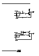
T89C51AC2 Figure 12. Column Latches Loading Procedure Column Latches Loading Save & Disable IT EA= 0 Column Latches Mapping FCON = 08h (FPS=1) Data Load DPTR= Address ACC= Data Exec: MOVX @DPTR, A Last Byte to load? Data memory Mapping FCON = 00h (FPS = 0) Restore IT Note: The last page address used when loading the column latch is the one used to select the page programming address. 9.3.
• Launch the programming by writing the data sequence 52h followed by A2h in FCON register (only from FM1). The end of the programming indicated by the FBUSY flag cleared. • Enable the interrupts. Figure 13.
T89C51AC2 Figure 14. Hardware Programming Procedure FLASH Spaces Programming Save & Disable IT EA= 0 Save & Disable IT EA= 0 FCON = 0Ch Launch Programming FCON= 54h FCON= A4h Data Load DPTR= 00h ACC= Data Exec: MOVX @DPTR, A FBusy Cleared? End Loading Restore IT Clear Mode FCON = 00h End Programming RestoreIT 9.3.7 Reading the FLASH Spaces User The following procedure is used to read the User space: • Read one byte in Accumulator by executing MOVC A,@A+DPTR with A+DPTR=read@.
Figure 15. Reading Procedure FLASH Spaces Reading FLASH Spaces Mapping FCON= 00000xx0b Data Read DPTR= Address ACC= 0 Exec: MOVC A, @A+DPTR Clear Mode FCON = 00h 9.3.8 Flash Protection from Parallel Programming The three lock bits in Hardware Security Byte (see "In-System Programming" section) are programmed according to Table 11 provide different level of protection for the onchip code and data located in FM0 and FM1. The only way to write this bits are the parallel mode.
T89C51AC2 9.4 Registers FCON RegisterFCON (S:D1h) FLASH Control Register 7 6 5 4 3 2 1 0 FPL3 FPL2 FPL1 FPL0 FPS FMOD1 FMOD0 FBUSY Bit Number Bit Mnemonic 7-4 FPL3:0 3 FPS 2-1 FMOD1:0 0 FBUSY Description Programming Launch Command Bits Write 5Xh followed by AXh to launch the programming according to FMOD1:0. (see Table 10.) FLASH Map Program Space Set to map the column latch space in the data memory space. Clear to re-map the data memory space. FLASH Mode See Table 9 or Table 10.
10. In-SystemProgramming (ISP) With the implementation of the User Space (FM0) and the Boot Space (FM1) in Flash technology the T89C51AC2 allows the system engineer the development of applications with a very high level of flexibility. This flexibility is based on the possibility to alter the customer program at any stages of a product’s life: • Before assembly the 1st personalization of the product by programming in the FM0 and if needed also a customized Boot loader in the FM1.
T89C51AC2 10.2 Boot Process 10.2.1 Software boot process example Many algorithms can be used for the software boot process. Before describing them, We give below the description of the different flags and bytes. Boot Loader Jump Bit (BLJB): - This bit indicates if on RESET the user wants to jump to this application at address @0000h on FM0 or execute the boot loader at address @F800h on FM1. - BLJB = 0 on parts delivered with bootloader programmed. - To read or modify this bit, the APIs are used.
Figure 17. Hardware Boot Process Algorithm bit ENBOOT in AUXR1 register is initialized with BLJB. RESET Hardware Hardware condition? No ENBOOT = 0 PC = 0000h Yes ENBOOT = 1 PC = F800h FCON = 00h FCON = F0h BLJB == 0 ? No Yes Software ENBOOT = 1 PC = F800h 10.3 ApplicationProgramming-Interface Application in FM0 Boot Loader in FM1 Several Application Program Interface (API) calls are available for use by an application program to permit selective erasing and programming of FLASH pages.
T89C51AC2 Table 12.
10.5 Hardware Security Byte Table 14. Hardware Security byte 7 6 5 4 3 2 1 0 X2B BLJB - - - LB2 LB1 LB0 Bit Number Bit Mnemonic 7 X2B X2 Bit Set this bit to start in standard mode Clear this bit to start in X2 mode. 6 BLJB Boot Loader JumpBit - 1: To start the user’s application on next RESET (@0000h) located in FM0, - 0: To start the boot loader(@F800h) located in FM1. 5-3 - 2-0 LB2:0 Description Reserved The value read from these bits are indeterminate.
T89C51AC2 11. Serial I/O Port The T89C51AC2 I/O serial port is compatible with the I/O serial port in the 80C52. It provides both synchronous and asynchronous communication modes. It operates as a Universal Asynchronous Receiver and Transmitter (UART) in three full-duplex modes (Modes 1, 2 and 3).
valid stop bits cannot clear the FE bit. When the FE feature is enabled, RI rises on the stop bit instead of the last data bit (See Figure 20. and Figure 21.). Figure 20. UART Timing in Mode 1 RXD D0 D1 D2 Start bit D3 D4 D5 D6 D7 Stop bit Data byte RI SMOD0=X FE SMOD0=1 Figure 21. UART Timing in Modes 2 and 3 RXD D0 Start bit D1 D2 D3 D4 Data byte D5 D6 D7 D8 Ninth Stop bit bit RI SMOD0=0 RI SMOD0=1 FE SMOD0=1 11.
T89C51AC2 more slaves at a time. The following example illustrates how a given address is formed. To address a device by its individual address, the SADEN mask byte must be 1111 1111b.
11.5 Registers Table 15. SCON Register SCON (S:98h) Serial Control Register 7 6 5 4 3 2 1 0 FE/SM0 SM1 SM2 REN TB8 RB8 TI RI Bit Number Bit Mnemonic 7 FE Description Framing Error bit (SMOD0=1) Clear to reset the error state, not cleared by a valid stop bit. Set by hardware when an invalid stop bit is detected. SM0 Serial port Mode bit 0 (SMOD0=0) Refer to SM1 for serial port mode selection.
T89C51AC2 Table 16. SADEN Register SADEN (S:B9h) Slave Address Mask Register 7 6 Bit Number Bit Mnemonic 7-0 5 4 3 2 1 0 2 1 0 2 1 0 Description Mask Data for Slave Individual Address Reset Value = 0000 0000b Not bit addressable Table 17. SADDR Register SADDR (S:A9h) Slave Address Register 7 6 Bit Number Bit Mnemonic 7-0 5 4 3 Description Slave Individual Address Reset Value = 0000 0000b Not bit addressable Table 18.
Table 19. PCON Register PCON (S:87h) Power Control Register 7 6 5 4 3 2 1 0 SMOD1 SMOD0 - POF GF1 GF0 PD IDL Bit Number Bit Mnemonic 7 SMOD1 Serial port Mode bit 1 Set to select double baud rate in mode 1, 2 or 3. 6 SMOD0 Serial port Mode bit 0 Clear to select SM0 bit in SCON register. Set to select FE bit in SCON register. 5 - Description Reserved The value read from this bit is indeterminate. Do not set this bit. 4 POF Power-Off Flag Clear to recognize next reset type.
T89C51AC2 12. Timers/Counters The T89C51AC2 implements two general-purpose, 16-bit Timers/Counters. Such are identified as Timer 0 and Timer 1, and can be independently configured to operate in a variety of modes as a Timer or an event Counter. When operating as a Timer, the Timer/Counter runs for a programmed length of time, then issues an interrupt request. When operating as a Counter, the Timer/Counter counts negative transitions on an external pin.
Figure 22. Timer/Counter x (x= 0 or 1) in Mode 0 see section “Clock” FTx CLOCK ÷6 0 THx (8 bits) 1 TLx (5 bits) Overflow TFx TCON reg Tx Timer x Interrupt Request C/Tx# TMOD reg INTx# GATEx TRx TMOD reg 12.2.2 Mode 1 (16-bit Timer) TCON reg Mode 1 configures Timer 0 as a 16-bit Timer with TH0 and TL0 registers connected in cascade (see Figure 23). The selected input increments TL0 register. Figure 23.
T89C51AC2 12.2.4 Mode 3 (Two 8-bit Timers) Mode 3 configures Timer 0 such that registers TL0 and TH0 operate as separate 8-bit Timers (see Figure 25). This mode is provided for applications requiring an additional 8bit Timer or Counter. TL0 uses the Timer 0 control bits C/T0# and GATE0 in TMOD register, and TR0 and TF0 in TCON register in the normal manner. TH0 is locked into a Timer function (counting FPER /6) and takes over use of the Timer 1 interrupt (TF1) and run control (TR1) bits.
12.3.1 Mode 0 (13-bit Timer) Mode 0 configures Timer 1 as a 13-bit Timer, which is set up as an 8-bit Timer (TH1 register) with a modulo-32 prescaler implemented with the lower 5 bits of the TL1 register (see Figure 22). The upper 3 bits of TL1 register are ignored. Prescaler overflow increments TH1 register. 12.3.2 Mode 1 (16-bit Timer) Mode 1 configures Timer 1 as a 16-bit Timer with TH1 and TL1 registers connected in cascade (see Figure 23). The selected input increments TL1 register. 12.3.
T89C51AC2 12.5 Registers Table 20. TCON Register TCON (S:88h) Timer/Counter Control Register 7 6 5 4 3 2 1 0 TF1 TR1 TF0 TR0 IE1 IT1 IE0 IT0 Bit Number Bit Mnemonic 7 TF1 Timer 1 Overflow Flag Cleared by hardware when processor vectors to interrupt routine. Set by hardware on Timer/Counter overflow, when Timer 1 register overflows. 6 TR1 Timer 1 Run Control Bit Clear to turn off Timer/Counter 1. Set to turn on Timer/Counter 1.
Table 21. TMOD Register TMOD (S:89h) Timer/Counter Mode Control Register. 7 6 5 4 3 2 1 0 GATE1 C/T1# M11 M01 GATE0 C/T0# M10 M00 Bit Number Bit Mnemonic 7 GATE1 Timer 1 Gating Control Bit Clear to enable Timer 1 whenever TR1 bit is set. Set to enable Timer 1 only while INT1# pin is high and TR1 bit is set. 6 C/T1# Timer 1 Counter/Timer Select Bit Clear for Timer operation: Timer 1 counts the divided-down system clock.
T89C51AC2 Table 22. TH0 Register TH0 (S:8Ch) Timer 0 High Byte Register 7 6 Bit Number Bit Mnemonic 7:0 5 4 3 2 1 0 2 1 0 2 1 0 Description High Byte of Timer 0. Reset Value= 0000 0000b Table 23. TL0 Register TL0 (S:8Ah) Timer 0 Low Byte Register 7 6 Bit Number Bit Mnemonic 7:0 5 4 3 Description Low Byte of Timer 0. Reset Value= 0000 0000b Table 24. TH1 Register TH1 (S:8Dh) Timer 1 High Byte Register 7 6 Bit Number Bit Mnemonic 7:0 5 4 3 Description High Byte of Timer 1.
Table 25. TL1 Register TL1 (S:8Bh) Timer 1 Low Byte Register 7 6 Bit Number Bit Mnemonic 7:0 5 4 3 2 1 0 Description Low Byte of Timer 1. Reset Value= 0000 0000b 58 T89C51AC2 Rev.
T89C51AC2 13. Timer 2 The T89C51AC2 timer 2 is compatible with timer 2 in the 80C52. It is a 16-bit timer/counter: the count is maintained by two eight-bit timer registers, TH2 and TL2 that are cascade- connected. It is controlled by T2CON register (See Table ) and T2MOD register (See Table 28). Timer 2 operation is similar to Timer 0 and Timer 1. C/T2 selects F T2 clock/6 (timer operation) or external pin T2 (counter operation) as timer clock.
Figure 27. Auto-Reload Mode Up/Down Counter see section “Clock” FT2 CLOCK :6 0 1 TR2 T2CON.2 CT/2 T2CON.1 T2 (DOWN COUNTING RELOAD VALUE) FFh (8-bit) FFh (8-bit) T2EX: 1=UP 2=DOWN TOGGLE T2CONreg EXF2 TL2 (8-bit) TH2 (8-bit) TIMER 2 INTERRUPT TF2 T2CONreg RCAP2L (8-bit) RCAP2H (8-bit) (UP COUNTING RELOAD VALUE) 13.2 Programmable Clock-Output In clock-out mode, timer 2 operates as a 50%-duty-cycle, programmable clock generator (See Figure 28).
T89C51AC2 It is possible to use timer 2 as a baud rate generator and a clock generator simultaneously. For this configuration, the baud rates and clock frequencies are not independent since both functions use the values in the RCAP2H and RCAP2L registers. Figure 28. Clock-Out Mode FT2 CLOCK 0 1 TR2 T2CON.2 CT/2 TL2 (8-bit) TH2 (8-bit) T2CON.1 OVERFLOW RCAP2L RCAP2H (8-bit) (8-bit) T2 1 0 :2 C/T2 T2OE T2CON reg T2MOD reg T2EX EXF2 EXEN2 T2CON reg TIMER 2 INTERRUPT T2CON reg 61 Rev.
13.3 Registers Table 26. T2CON Register T2CON (S:C8h) Timer 2 Control Register 7 6 5 4 3 2 1 0 TF2 EXF2 RCLK TCLK EXEN2 TR2 C/T2# CP/RL2# Bit Number Bit Mnemonic 7 TF2 Description Timer 2 overflow Flag TF2 is not set if RCLK=1 or TCLK = 1. Must be cleared by software. Set by hardware on timer 2 overflow. 6 EXF2 Timer 2 External Flag Set when a capture or a reload is caused by a negative transition on T2EX pin if EXEN2=1.
T89C51AC2 Table 27. T2MOD Register T2MOD (S:C9h) Timer 2 Mode Control Register 7 6 5 4 3 2 1 0 - - - - - - T2OE DCEN Bit Number Bit Mnemonic 7 - Reserved The value read from this bit is indeterminate. Do not set this bit. 6 - Reserved The value read from this bit is indeterminate. Do not set this bit. 5 - Reserved The value read from this bit is indeterminate. Do not set this bit. 4 - Reserved The value read from this bit is indeterminate. Do not set this bit.
Table 29. TL2 Register TL2 (S:CCh) Timer 2 Low Byte Register 7 6 5 4 3 2 1 0 - - - - - - - - Bit Number Bit Mnemonic 7-0 Description Low Byte of Timer 2. Reset Value = 0000 0000b Not bit addressable Table 30. RCAP2H Register RCAP2H (S:CBh) Timer 2 Reload/Capture High Byte Register 7 6 5 4 3 2 1 0 - - - - - - - - Bit Number Bit Mnemonic 7-0 Description High Byte of Timer 2 Reload/Capture. Reset Value = 0000 0000b Not bit addressable Table 31.
T89C51AC2 14. WatchDog Timer T89C51AC2 contains a powerful programmable hardware WatchDog Timer (WDT) that automatically resets the chip if it software fails to reset the WDT before the selected time interval has elapsed. It permits large Time-Out ranking from 16ms to 2s @Fosc = 12MHz in X1 mode. This WDT consists of a 14-bit counter plus a 7-bit programmable counter, a WatchDog Timer reset register (WDTRST) and a WatchDog Timer programming (WDTPRG) register.
14.1 WatchDog Programming The three lower bits (S0, S1, S2) located into WDTPRG register permit to program the WDT duration. Table 32.
T89C51AC2 14.2 WatchDog Timer during Power down mode and Idle In Power Down mode the oscillator stops, which means the WDT also stops. While in Power Down mode, the user does not need to service the WDT. There are 2 methods of exiting Power Down mode: by a hardware reset or via a level activated external interrupt which is enabled prior to entering Power Down mode. When Power Down is exited with hardware reset, the watchdog is disabled. Exiting Power Down with an interrupt is significantly different.
Table 35. WDTRST Register WDTRST (S:A6h Write only) WatchDog Timer Enable register 7 6 5 4 3 2 1 0 - - - - - - - - Bit Number Bit Mnemonic 7 - Description Watchdog Control Value Reset Value = 1111 1111b Note: 68 The WDRST register is used to reset/enable the WDT by writing 1EH then E1H in sequence without instruction between these two sequences. T89C51AC2 Rev.
T89C51AC2 15. Programmable Counter Array PCA The PCA provides more timing capabilities with less CPU intervention than the standard timer/counters. Its advantages include reduced software overhead and improved accuracy. The PCA consists of a dedicated timer/counter which serves as the time base for an array of five compare/capture modules.
Figure 30. PCA Timer/Counter To PCA modules FPca/6 overflow FPca / 2 CH T0 OVF It CL 16 bit up/down counter P1.2 CIDL WDTE CF CR CPS1 CPS0 ECF CMOD 0xD9 Idle CCF4 CCF3 CCF2 CCF1 CCF0 CCON 0xD8 The CMOD register includes three additional bits associated with the PCA. • The CIDL bit which allows the PCA to stop during idle mode. • The WDTE bit which enables or disables the watchdog function on module 4.
T89C51AC2 Each module in the PCA has a special function register associated with it (CCAPM0 for module 0 ...). The CCAPM0:4 registers contain the bits that control the mode that each module will operate in. 15.3 PCA Interrupt • The ECCF bit enables the CCF flag in the CCON register to generate an interrupt when a match or compare occurs in the associated module. • The PWM bit enables the pulse width modulation mode.
Figure 32. PCA Capture Mode PCA Counter CH (8bits) CL (8bits) CEXn n = 0, 4 CCAPnH CCAPnL PCA Interrupt Request CCFn CCON - 0CAPPnCAPNn000ECCFn 0 7 CCAPMn Register (n = 0, 4) 15.5 16-bit Software Timer Mode The PCA modules can be used as software timers by setting both the ECOM and MAT bits in the modules CCAPMn register.
T89C51AC2 15.6 High Speed Output Mode In this mode the CEX output (on port 1) associated with the PCA module will toggle each time a match occurs between the PCA counter and the module’s capture registers. To activate this mode the TOG, MAT, and ECOM bits in the module’s CCAPMn SFR must be set. Figure 34.
Figure 35. PCA PWM Mode CCAPnH CL rolls over from FFh TO 00h loads CCAPnH contents into CCAPnL CCAPnL “0” CL < CCAPnL CL (8 bits) 8-Bit Comparator CEX CL >= CCAPnL “1” 15.8 PCA Watchdog Timer ECOMn PWMn CCAPMn.6 CCAPMn.1 An on-board watchdog timer is available with the PCA to improve system reliability without increasing chip count. Watchdog timers are useful for systems that are sensitive to noise, power glitches, or electrostatic discharge.
T89C51AC2 15.9 PCA Registers Table 36. CMOD Register CMOD (S:D8h) PCA Counter Mode Register 7 6 5 4 3 2 1 0 CIDL WDTE - - - CPS1 CPS0 ECF Bit Number Bit Mnemonic 7 CIDL 6 WDTE 5 - Reserved The value read from this bit is indeterminate. Do not set this bit. 4 - Reserved The value read from this bit is indeterminate. Do not set this bit. 3 - Reserved The value read from this bit is indeterminate. Do not set this bit.
Table 37. CCON Register CCON (S:D8h) PCA Counter Control Register 7 6 5 4 3 2 1 0 CF CR - CCF4 CCF3 CCF2 CCF1 CCF0 Bit Number Bit Mnemonic 7 CF PCA Timer/Counter Overflow flag Set by hardware when the PCA Timer/Counter rolls over. This generates a PCA interrupt request if the ECF bit in CMOD register is set. Must be cleared by software. 6 CR PCA Timer/Counter Run Control bit Clear to turn the PCA Timer/Counter off. Set to turn the PCA Timer/Counter on.
T89C51AC2 Table 38. CCAPnH Registers CCAP0H (S:FAh) CCAP1H (S:FBh) CCAP2H (S:FCh) CCAP3H (S:FDh) CCAP4H (S:FEh) PCA High Byte Compare/Capture Module n Register (n=0..4) 7 6 5 4 3 2 1 0 CCAPnH 7 CCAPnH 6 CCAPnH 5 CCAPnH 4 CCAPnH 3 CCAPnH 2 CCAPnH 1 CCAPnH 0 Bit Number Bit Mnemonic 7:0 CCAPnH 7:0 Description High byte of EWC-PCA comparison or capture values Reset Value = 0000 0000b Table 39.
Table 40. CCAPMn Registers CCAPM0 (S:DAh) CCAPM1 (S:DBh) CCAPM2 (S:DCh) CCAPM3 (S:DDh) CCAPM4 (S:DEh) PCA Compare/Capture Module n Mode registers (n=0..4) 7 6 5 4 3 2 1 0 - ECOMn CAPPn CAPNn MATn TOGn PWMn ECCFn Bit Number Bit Mnemonic 7 - Description Reserved The Value read from this bit is indeterminate. Do not set this bit. 6 ECOMn Enable Compare Mode Module x bit Clear to disable the Compare function. Set to enable the Compare function.
T89C51AC2 Table 41. CH Register CH (S:F9h) PCA Counter Register High value 7 6 5 4 3 2 1 0 CH 7 CH 6 CH 5 CH 4 CH 3 CH 2 CH 1 CH 0 Bit Number Bit Mnemonic 7:0 CH 7:0 Description High byte of Timer/Counter Reset Value = 0000 00000b Table 42. CL Register CL (S:E9h) PCA counter Register Low value 7 6 5 4 3 2 1 0 CL 7 CL 6 CL 5 CL 4 CL 3 CL 2 CL 1 CL 0 Bit Number Bit Mnemonic 7:0 CL0 7:0 Description Low byte of Timer/Counter Reset Value = 0000 00000b 79 Rev.
16. Analog-to-Digital Converter (ADC) This section describes the on-chip 10 bit analog-to-digital converter of the T89C51AC2. Eight ADC channels are available for sampling of the external sources AN0 to AN7. An analog multiplexer allows the single ADC converter to select one from the 8 ADC channels as ADC input voltage (ADCIN). ADCIN is converted by the 10 bit-cascaded potentiometric ADC. Two kind of conversion are available: - Standard conversion (8 bits). - Precision conversion (10 bits).
T89C51AC2 Figure 36. ADC Description ADCON.5 ADCON.3 ADEN ADSST ADC Interrupt Request ADCON.4 ADEOC ADC CLOCK CONTROL EADC AN0/P1.0 000 AN1/P1.1 001 AN2/P1.2 010 AN3/P1.3 011 AN4/P1.4 100 AN5/P1.5 101 AN6/P1.6 110 AN7/P1.7 111 IEN1.1 ADCIN 8 ADDH 2 ADDL + SAR - AVSS Sample and Hold 10 R/2R DAC SCH2 SCH1 SCH0 ADCON.2 ADCON.1 ADCON.0 VAREF VAGND Figure 37 shows the timing diagram of a complete conversion.
16.3 ADC Converter Operation A start of single A/D conversion is triggered by setting bit ADSST (ADCON.3). After completion of the A/D conversion, the ADSST bit is cleared by hardware. The end-of-conversion flag ADEOC (ADCON.4) is set when the value of conversion is available in ADDH and ADDL, it must be cleared by software. If the bit EADC (IEN1.1) is set, an interrupt occur when flag ADEOC is set (see Figure 39). Clear this flag for rearming the interrupt.
T89C51AC2 16.6 ADC Standby Mode When the ADC is not used, it is possible to set it in standby mode by clearing bit ADEN in ADCON register. In this mode its power dissipation is about 1uW. 16.7 IT ADC management An interrupt end-of-conversion will occurs when the bit ADEOC is activated and the bit EADC is set. For re-arming the interrupt the bit ADEOC must be cleared by software. Figure 39. ADC interrupt structure ADCI ADEOC ADCON.2 EADC IEN1.1 16.8 Routines examples 1. Configure P1.2 and P1.
16.9 Registers Table 44. ADCF Register ADCF (S:F6h) ADC Configuration 7 6 5 4 3 2 1 0 CH 7 CH 6 CH 5 CH 4 CH 3 CH 2 CH 1 CH 0 Bit Number Bit Mnemonic 7-0 CH 0:7 Description Channel Configuration Set to use P1.x as ADC input. Clear to use P1.x as standart I/O port. Reset Value=0000 0000b Table 45.
T89C51AC2 Table 46. ADCLK Register ADCLK (S:F2h) ADC Clock Prescaler 7 6 5 4 3 2 1 0 - - - PRS 4 PRS 3 PRS 2 PRS 1 PRS 0 Bit Number Bit Mnemonic 7-5 - 4-0 PRS4:0 Description Reserved The value read from these bits are indeterminate. Do not set these bits. Clock Prescaler fADC = fcpu clock/ (4 (or 2 in X2 mode)* (PRS +1)) Reset Value: XXX0 0000b Table 47.
17. Interrupt System The controller has a total of 8 interrupt vectors: two external interrupts (INT0 and INT1), three timer interrupts (timers 0, 1 and 2), a serial port interrupt, a PCA, a timer overrun interrupt and an ADC. These interrupts are shown below. Figure 40. Interrupt Control System INT0# 00 01 10 11 External Interrupt 0 Highest Priority Interrupts EX0 IEN0.0 Timer 0 00 01 10 11 ET0 INT1# External Interrupt 1 IEN0.1 00 01 10 11 EX1 IEN0.
T89C51AC2 Each of the interrupt sources can be individually enabled or disabled by setting or clearing a bit in the Interrupt Enable register. This register also contains a global disable bit which must be cleared to disable all the interrupts at the same time. Each interrupt source can also be individually programmed to one of four priority levels by setting or clearing a bit in the Interrupt Priority registers. The Table below shows the bit values and priority levels associated with each combination.
17.1 Registers Table 51. IEN0 Register IEN0 (S:A8h) Interrupt Enable Register 7 6 5 4 3 2 1 0 EA EC ET2 ES ET1 EX1 ET0 EX0 Bit Number Bit Mnemonic Description 7 EA Enable All interrupt bit Clear to disable all interrupts. Set to enable all interrupts. If EA=1, each interrupt source is individually enabled or disabled by setting or clearing its interrupt enable bit. 6 EC PCA Interrupt Enable Clear to disable the PCA interrupt. Set to enable the PCA interrupt.
T89C51AC2 Table 52. IEN1 Register IEN1 (S:E8h) Interrupt Enable Register 7 6 5 4 3 2 1 0 - - - - - EADC - Bit Number Bit Mnemonic 7 - Reserved The value read from this bit is indeterminate. Do not set this bit. 6 - Reserved The value read from this bit is indeterminate. Do not set this bit. 5 - Reserved The value read from this bit is indeterminate. Do not set this bit. 4 - Reserved The value read from this bit is indeterminate. Do not set this bit.
Table 53. IPL0 Register IPL0 (S:B8h) Interrupt Enable Register 7 6 5 4 3 2 1 0 - PPC PT2 PS PT1 PX1 PT0 PX0 Bit Number Bit Mnemonic 7 - 6 PPC PCA Interrupt Priority bit Refer to PPCH for priority level 5 PT2 Timer 2 overflow interrupt Priority bit Refer to PT2H for priority level. 4 PS Serial port Priority bit Refer to PSH for priority level. 3 PT1 Timer 1 overflow interrupt Priority bit Refer to PT1H for priority level.
T89C51AC2 Table 54. IPL1 Register IPL1 (S:F8h) Interrupt Priority Low Register 1 7 6 5 4 3 2 1 0 - - - - - PADCL - Bit Number Bit Mnemonic 7 - Reserved The value read from this bit is indeterminate. Do not set this bit. 6 - Reserved The value read from this bit is indeterminate. Do not set this bit. 5 - Reserved The value read from this bit is indeterminate. Do not set this bit. 4 - Reserved The value read from this bit is indeterminate. Do not set this bit.
Table 55. IPL0 Register IPH0 (B7h) Interrupt High Priority Register 7 6 5 4 3 2 1 0 - PPCH PT2H PSH PT1H PX1H PT0H PX0H Bit Number Bit Mnemonic 7 - 6 5 4 3 2 1 0 PPCH Description Reserved The value read from this bit is indeterminate. Do not set this bit.
T89C51AC2 Table 56. IPH1 Register IPH1 (S:FFh) Interrupt high priority Register 1 7 6 5 4 - - - - Bit Number Bit Mnemonic 7 - Reserved The value read from this bit is indeterminate. Do not set this bit. 6 - Reserved The value read from this bit is indeterminate. Do not set this bit. 5 - Reserved The value read from this bit is indeterminate. Do not set this bit. 4 - Reserved The value read from this bit is indeterminate. Do not set this bit.
18. Electrical Characteristics 18.1 Absolute Maximum Ratings (1) Note: Ambiant Temperature Under Bias: I = industrial.................................................-40°C to 85°C Storage Temperature ............................-65°C to + 150°C Voltage on VCC from V SS..........................................-0.5 V to + 6V Voltage on Any Pin from VSS............-0.5 V to VCC + 0.2 V Stresses at or above those listed under “Absolute Maximum Ratings” may cause permanent damage to the device.
T89C51AC2 Symbol Parameter ITL Logical 1 to 0 Transition Current, ports 1, 2, 3 and 4 CIO Capacitance of I/O Buffer IPD Power Down Current Min Typ(5) Max -650 160 Unit Test Conditions µA Vin = 2.0 V 10 pF Fc = 1 MHz TA = 25°C 350 µA 4.5V < VCC < 5.5V(3) Power Supply Current ICC ICCOP = 0.7 Freq (MHz) + 3 mA ICCIDLE = 0.6 Freq (MHz) + 2 mA Notes: 1. Operating ICC is measured with all output pins disconnected; XTAL1 driven with TCLCH, TCHCL = 5 ns (see Figure 44.), VIL = VSS + 0.
Figure 41. ICC Test Condition, Active Mode VCC ICC VCC VCC P0 VCC RST EA XTAL2 XTAL1 (NC) CLOCK SIGNAL VSS All other pins are disconnected. Figure 42. ICC Test Condition, Idle Mode VCC ICC VCC VCC P0 RST EA XTAL2 XTAL1 (NC) CLOCK SIGNAL VSS All other pins are disconnected. Figure 43. ICC Test Condition, Power-Down Mode VCC ICC VCC VCC P0 RST (NC) EA XTAL2 XTAL1 VSS All other pins are disconnected. 96 T89C51AC2 Rev.
T89C51AC2 Figure 44. Clock Signal Waveform for ICC Tests in Active and Idle Modes VCC-0.5V 0.45V TCLCH TCHCL TCLCH = TCHCL = 5ns. 0.7VCC 0.2VCC-0.1 18.3 DC Parameters for A/D Converter Table 58. DC Parameters for AD Converter in Precision conversion Symbol Parameter Min Typ(1) Max Vref + Analog input voltage Rref Resistance between Vref and Vss Vref Reference voltage Cai Analog input Capacitance 60 INL Integral non linearity 1 2 lsb DNL Differential non linearity 0.
18.4.2 External Program Memory Characteristics Table 59. Symbol Description Symbol T Parameter Oscillator clock period TLHLL ALE pulse width TAVLL Address Valid to ALE TLLAX Address Hold After ALE TLLIV ALE to Valid Instruction In TLLPL ALE to PSEN TPLPH PSEN Pulse Width TPLIV PSEN to Valid Instruction In TPXIX Input Instruction Hold After PSEN TPXIZ Input Instruction Float After PSEN TAVIV Address to Valid Instruction In TPLAZ PSEN Low to Address Float Table 60.
T89C51AC2 Table 61. AC Parameters for a Variable Clock Symbol Type Standard Clock X2 Clock X parameter Units TLHLL Min 2T-x T-x 10 ns TAVLL Min T-x 0.5 T - x 15 ns TLLAX Min T-x 0.5 T - x 15 ns TLLIV Max 4T-x 2T-x 30 ns TLLPL Min T-x 0.5 T - x 10 ns TPLPH Min 3T-x 1.5 T - x 20 ns TPLIV Max 3T-x 1.5 T - x 40 ns TPXIX Min x x 0 ns TPXIZ Max T-x 0.5 T - x 7 ns TAVIV Max 5T-x 2.5 T - x 40 ns TPLAZ Max x x 10 ns 18.4.
18.4.4 External Data Memory Characteristics Table 62. Symbol Description Symbol Parameter TRLRH RD Pulse Width TWLWH WR Pulse Width TRLDV RD to Valid Data In TRHDX Data Hold After RD TRHDZ Data Float After RD TLLDV ALE to Valid Data In TAVDV Address to Valid Data In TLLWL ALE to WR or RD TAVWL Address to WR or RD TQVWX Data Valid to WR Transition TQVWH Data set-up to WR High TWHQX Data Hold After WR TRLAZ RD Low to Address Float TWHLH RD or WR High to ALE high Table 63.
T89C51AC2 Table 64. AC Parameters for a Variable Clock Symbol Type Standard Clock X2 Clock X parameter Units TRLRH Min 6T-x 3T-x 20 ns TWLWH Min 6T-x 3T-x 20 ns TRLDV Max 5T-x 2.5 T - x 25 ns TRHDX Min x x 0 ns TRHDZ Max 2T-x T-x 20 ns TLLDV Max 8T-x 4T -x 40 ns TAVDV Max 9T-x 4.5 T - x 60 ns TLLWL Min 3T-x 1.5 T - x 25 ns TLLWL Max 3T+x 1.5 T + x 25 ns TAVWL Min 4T-x 2T-x 25 ns TQVWX Min T-x 0.5 T - x 15 ns TQVWH Min 7T-x 3.
18.4.6 External Data Memory Read Cycle TWHLH TLLDV ALE PSEN TLLWL TRLRH RD TRHDZ TAVDV TLLAX PORT 0 TRHDX A0-A7 DATA IN TRLAZ TAVWL PORT 2 18.4.7 Serial Port Timing Shift Register Mode ADDRESS OR SFR-P2 ADDRESS A8-A15 OR SFR P2 Table 65.
T89C51AC2 18.4.8 Shift Register Timing Waveforms 0 INSTRUCTION 1 2 3 4 5 6 7 8 ALE TXLXL CLOCK TXHQX TQVXH 0 OUTPUT DATA 1 2 INPUT DATA 4 5 6 TXHDX TXHDV WRITE to SBUF 3 VALID VALID VALID SET TI VALID VALID VALID VALID Table 68. AC Parameters Symbol Parameter Min Max Units TCLCL Oscillator Period 25 ns TCHCX High Time 5 ns TCLCX Low Time 5 ns TCLCH Rise Time 5 ns TCHCL Fall Time 5 ns 60 % TCHCX/TCLCX 18.4.
18.4.12 Float Waveforms FLOAT VOH - 0.1 V VOL + 0.1 V VLOAD VLOAD + 0.1 V VLOAD - 0.1 V For timing purposes as port pin is no longer floating when a 100 mV change from load voltage occurs and begins to float when a 100 mV change from the loaded VOH/V OL level occurs. IOL/IOH ≥ ± 20mA. 18.4.13 Clock Waveforms 104 Valid in normal clock mode. In X2 mode XTAL2 must be changed to XTAL2/2. T89C51AC2 Rev.
T89C51AC2 INTERNAL CLOCK STATE4 STATE5 STATE6 STATE1 STATE2 STATE3 STATE4 STATE5 P1 P1 P1 P1 P1 P1 P1 P1 P2 P2 P2 P2 P2 P2 P2 P2 XTAL2 ALE THESE SIGNALS ARE NOT ACTIVATED DURING THE EXECUTION OF A MOVX INSTRUCTION EXTERNAL PROGRAM MEMORY FETCH PSEN P0 DATA SAMPLED PCL OUT DATA SAMPLED FLOAT P2 (EXT) PCL OUT FLOAT DATA SAMPLED PCL OUT FLOAT INDICATES ADDRESS TRANSITIONS READ CYCLE RD PCL OUT (IF PROGRAM MEMORY IS EXTERNAL) DPL OR Rt OUT P0 P2 DATA SAMPLED FLOAT INDIC
18.5.14 Flash Memory Table 69. Timing Symbol Definitions Signals Conditions S(Hardware condition) PSEN#,EA L Low R RST V Valid B FBUSY flag X No Longer Valid Table 70. Memory AC Timing VDD= 5 V +/- 10% , TA= -40 to +85°C Symbol Parameter Min Typ Max Unit TSVRL Input PSEN# Valid to RST Edge 50 ns TRLSX Input PSEN# Hold after RST Edge 50 ns TBHBL FLASH Internal Busy (Programming) Time 10 ms Figure 45. FLASH Memory - ISP Waveforms RST TSVRL TRLSX PSEN#1 Figure 46.
T89C51AC2 19. Ordering Information Table 71. Possible order entries Part Number Memory Size Supply Voltage Temperature Range Max Frequency Package Packing T89C51AC2-RLTIM 32 Kbytes 5V + 10% Industrial 40 MHz VQFP44 Tray T89C51AC2-SLSIM 32 Kbytes 5V + 10% Industrial 40 MHz PLCC44 Stick 107 Rev.
T89C51AC2 Table of Contents 1. Features ......................................................................................................... 1 2. Description ...................................................................................................... 1 3. Block Diagram ................................................................................................. 2 4. Pin Configuration ............................................................................................. 3 4.
14.1 WatchDog Programming ......................................................................... 66 14.2 WatchDog Timer during Power down mode and Idle .............................. 67 15. Programmable Counter Array PCA ............................................................... 69 15.1 PCA Timer ............................................................................................... 69 15.2 PCA modules ..........................................................................................
Atmel Headquarters Atmel Operations Corporate Headquarters Memory 2325 Orchard Parkway San Jose, CA 95131 TEL (408) 441-0311 FAX (408) 487-2600 Europe Atmel SarL Route des Arsenaux 41 Casa Postale 80 CH-1705 Fribourg Switzerland TEL (41) 26-426-5555 FAX (41) 26-426-5500 Asia Atmel Asia, Ltd. Room 1219 Chinachem Golden Plaza 77 Mody Road Tsimhatsui East Kowloon Hong Kong TEL (852) 2721-9778 FAX (852) 2722-1369 Japan Atmel Japan K.K. 9F, Tonetsu Shinkawa Bldg.