T89C51RD2 0 to 40MHz Flash Programmable 8-bit Microcontroller 1. Description ATMEL Wireless and Microcontrollers T89C51RD2 is high performance CMOS Flash version of the 80C51 CMOS single chip 8-bit microcontroller. It contains a 64 Kbytes Flash memory block for program and for data. The 64 Kbytes Flash memory can be programmed either in parallel mode or in serial mode with the ISP capability or with software. The programming voltage is internally generated from the standard VCC pin.
T89C51RD2 • Power supply: - M version: Commercial and industrial 4.5V to 5.5V : 40MHz X1 Mode, 20MHz X2 Mode 3V to 5.5V : 33MHz X1 Mode, 16 MHz X2 Mode - L version: Commercial and industrial 2.7V to 3.6V : 25MHz X1 Mode, 12MHz X2 Mode Temperature ranges: Commercial (0 to +70°C) and industrial (-40 to +85°C). • • Packages: PDIL40, PLCC44, VQFP44, PLCC68, VQFP64 Table 1. Memory Size PDIL40 PLCC44 Flash (bytes) EEPROM (bytes) XRAM (bytes) TOTAL RAM (bytes) I/O 64k 2k 1024 1280 32 VQFP44 1.
T89C51RD2 4.
T89C51RD2 reserved 4 Rev.
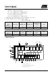
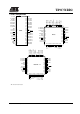
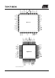
T89C51RD2 6 7 8 31 30 EA ALE/PROG PSEN P2.7/AD15 P2.6/AD14 P2.5/AD13 P3.6/WR 16 25 P3.7/RD XTAL2 17 18 19 20 24 XTAL1 P0.6/AD6 RST 10 36 P0.7/AD7 P3.0/RxD 35 34 33 EA P3.1/TxD 11 12 13 P2.4/AD12 P2.3/AD11 P3.2/INT0 P3.3/INT1 14 15 32 31 PSEN P2.2/AD10 P3.4/T0 P3.5/T1 16 30 P2.6/A14 17 29 P2.5/A13 NIC* P2.1/AD9 PLCC NIC* ALE/PROG P2.7/A15 P0.3/AD3 P0.2/AD2 P0.1/AD1 P0.0/AD0 VCC VSS1/NIC* P1.0/T2 P1.1/T2EX P1.2/ECI P1.3/CEX0 P1.4/CEX1 P0.
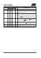
ALE/PROG P5.1 P2.5/A13 1 68 67 66 65 64 63 62 61 P5.2 2 P2.6/A14 3 P2.7/A15 4 PSEN NIC EA P0.6/AD6 5 NIC P0.5/AD5 6 NIC P5.3 7 P0.7/AD7 P0.4/AD4 8 60 59 58 57 56 55 54 53 52 51 50 49 P5.0 P2.4/A12 P2.3/A11 P4.7 P2.2/A10 P2.1/A9 P2.0/A8 P4.6 48 47 46 45 44 27 28 29 30 31 32 33 34 35 36 37 38 39 40 41 42 43 XTAL2 P3.7/RD P4.4 P3.6/WR P4.3 VSS P4.5 XTAL1 P3.5/T1 P3.4/T0 P3.2/INT0 P3.3/INT1 NIC P3.1/TxD NIC NIC NIC P3.0/RxD NIC NIC NIC NIC P0.4/AD4 P5.4 P5.3 P0.5/AD5 P0.
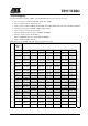
T89C51RD2 Pin Number Mnemonic Name and Function Type DIL LCC VQFP 1.4 20 22 16 I Ground: 0V reference 1 39 I Optional Ground: Contact the Sales Office for ground connection. 40 44 38 I Power Supply: This is the power supply voltage for normal, idle and powerdown operation P0.0-P0.7 39-32 43-36 37-30 I/O Port 0: Port 0 is an open-drain, bidirectional I/O port. Port 0 pins that have 1s written to them float and can be used as high impedance inputs.
T89C51RD2 Pin Number Mnemonic Type Name and Function DIL LCC VQFP 1.4 17 19 13 O Reset 9 10 4 I/O Reset: A high on this pin for two machine cycles while the oscillator is running, resets the device. An internal diffused resistor to VSS permits a power-on reset using only an external capacitor to VCC. This pin is an output when the hardware watchdog forces a system reset.
T89C51RD2 5.1. Pin Description for 64/68 pin Packages Port 4 and Port 5 are 8-bit bidirectional I/O ports with internal pull-ups. Pins that have 1 written to them are pulled high by the internal pull ups and can be used as inputs. As inputs, pins that are externally pulled low will source current because of the internal pull-ups. Refer to the previous pin description for other pins. VSS VCC P0.0 P0.1 P0.2 P0.3 P0.4 P0.5 P0.6 P0.7 P1.0 P1.1 P1.2 P1.3 P1.4 P1.5 P1.6 P1.7 P2.0 P2.1 P2.2 P2.3 P2.4 P2.5 P2.
T89C51RD2 6. Enhanced Features In comparison to the original 80C52, the T89C51RD2 implements some new features, which are: • • • • • • • • • • The X2 option. The Dual Data Pointer. The extended RAM. The Programmable Counter Array (PCA). The Watchdog. The 4 level interrupt priority system. The power-off flag. The ONCE mode. The ALE disabling. Some enhanced features are also located in the UART and the timer 2. 6.1.
T89C51RD2 XTAL1 XTAL1:2 X2 bit CPU clock STD Mode X2 Mode STD Mode Figure 2. Mode Switching Waveforms The X2 bit in the CKCON register (See Table 2.) allows to switch from 12 clock periods per instruction to 6 clock periods and vice versa. At reset, the standard speed is activated (STD mode). Setting this bit activates the X2 feature (X2 mode). The T0X2, T1X2, T2X2, SiX2, PcaX2 and WdX2 bits in the CKCON register (See Table 2.
T89C51RD2 Bit Number Bit Mnemonic Description 1 T0X2 Timer0 clock (This control bit is validated when the CPU clock X2 is set; when X2 is low, this bit has no effect) Clear to select 6 clock periods per peripheral clock cycle. Set to select 12 clock periods per peripheral clock cycle 0 X2 CPU clock Clear to select 12 clock periods per machine cycle (STD mode) for CPU and all the peripherals. Set to select 6clock periods per machine cycle (X2 mode) and to enable the individual peripherals "X2" bits.
T89C51RD2 6.2. Dual Data Pointer Register Ddptr The additional data pointer can be used to speed up code execution and reduce code size. The dual DPTR structure is a way by which the chip will specify the address of an external data memory location. There are two 16-bit DPTR registers that address the external memory, and a single bit called DPS = AUXR1/bit0 (See Table 3.) that allows the program code to switch between them (Refer to Figure 3).
T89C51RD2 ; Block move using dual data pointers ; Modifies DPTR0, DPTR1, A and PSW ; note: DPS exits opposite of entry state ; unless an extra INC AUXR1 is added ; 00A2 AUXR1 EQU 0A2H ; 0000 909000MOV DPTR,#SOURCE ; address of SOURCE 0003 05A2 INC AUXR1 ; switch data pointers 0005 90A000 MOV DPTR,#DEST ; address of DEST 0008 LOOP: 0008 05A2 INC AUXR1 ; switch data pointers 000A E0 MOVX A,@DPTR ; get a byte from SOURCE 000B A3 INC DPTR ; increment SOURCE address 000C 05A2 INC AUXR1 ; switch data pointers 000
T89C51RD2 6.3. Expanded RAM (XRAM) The T89C51RD2 provide additional Bytes of random access memory (RAM) space for increased data parameter handling and high level language usage. T89C51RD2 devices have expanded RAM in external data space; Maximum size and location are described in Table 4. Table 4. Description of expanded RAM Port Address XRAM size T89C51RD2 1024 Start End 00h 3FFh The T89C51RD2 has internal data memory that is mapped into four separate segments. The four segments are: • • • • 1.
T89C51RD2 • The XRAM bytes can be accessed by indirect addressing, with EXTRAM bit cleared and MOVX instructions. This part of memory which is physically located on-chip, logically occupies the first bytes of external data memory. The bits XRS0 and XRS1 are used to hide a part of the available XRAM as explained in Table . This can be useful if external peripherals are mapped at addresses already used by the internal XRAM.
T89C51RD2 6.4. Timer 2 The timer 2 in the T89C51RD2 is compatible with the timer 2 in the 80C52. It is a 16-bit timer/counter: the count is maintained by two eight-bit timer registers, TH2 and TL2, connected in cascade. It is controlled by T2CON register (See Table 5) and T2MOD register (See Table 6). Timer 2 operation is similar to Timer 0 and Timer 1. C/T2 selects FOSC/12 (timer operation) or external pin T2 (counter operation) as the timer clock input.
T89C51RD2 XTAL1 FXTAL :12 FOSC 0 1 T2 C/T2 T2CONreg TR2 T2CONreg (DOWN COUNTING RELOAD VALUE) FFh FFh (8-bit) (8-bit) T2EX: if DCEN=1, 1=UP if DCEN=1, 0=DOWN if DCEN = 0, up counting TOGGLE T2CONreg EXF2 TL2 TH2 (8-bit) (8-bit) TF2 TIMER 2 INTERRUPT T2CONreg RCAP2L (8-bit) RCAP2H (8-bit) (UP COUNTING RELOAD VALUE) Figure 5. Auto-Reload Mode Up/Down Counter (DCEN = 1) 6.4.2.
T89C51RD2 It is possible to use timer 2 as a baud rate generator and a clock generator simultaneously. For this configuration, the baud rates and clock frequencies are not independent since both functions use the values in the RCAP2H and RCAP2L registers. XTAL1 :2 TR2 T2CON reg TL2 (8-bit) TH2 (8-bit) OVEFLOW RCAP2L RCAP2H (8-bit) (8-bit) Toggle T2 Q D T2OE T2MOD reg T2EX EXF2 EXEN2 T2CON reg TIMER 2 INTERRUPT T2CON reg Figure 6. Clock-Out Mode C/T2 = 0 Rev.
T89C51RD2 Table 5. T2CON Register T2CON - Timer 2 Control Register (C8h) 7 6 5 4 3 2 1 0 TF2 EXF2 RCLK TCLK EXEN2 TR2 C/T2# CP/RL2# Bit Number Bit Mnemonic 7 TF2 6 EXF2 Timer 2 External Flag Set when a capture or a reload is caused by a negative transition on T2EX pin if EXEN2=1. When set, causes the CPU to vector to timer 2 interrupt routine when timer 2 interrupt is enabled. Must be cleared by software.
T89C51RD2 Table 6. T2MOD Register T2MOD - Timer 2 Mode Control Register (C9h) 7 6 5 4 3 2 1 0 - - - - - - T2OE DCEN Bit Number Bit Mnemonic 7 - Reserved The value read from this bit is indeterminate. Do not set this bit. 6 - Reserved The value read from this bit is indeterminate. Do not set this bit. 5 - Reserved The value read from this bit is indeterminate. Do not set this bit. 4 - Reserved The value read from this bit is indeterminate. Do not set this bit.
T89C51RD2 6.5. Programmable Counter Array PCA The PCA provides more timing capabilities with less CPU intervention than the standard timer/counters. Its advantages include reduced software overhead and improved accuracy. The PCA consists of a dedicated timer/ counter which serves as the time base for an array of five compare/ capture modules.
T89C51RD2 To PCA modules Fosc /12 overflow Fosc / 4 CH T0 OVF It CL 16 bit up/down counter P1.2 CIDL WDTE CF CR CPS1 CPS0 ECF CMOD 0xD9 CCF2 CCF1 CCF0 CCON 0xD8 Idle CCF4 CCF3 Figure 7. PCA Timer/Counter Table 7. CMOD: PCA Counter Mode Register CMOD Address 0D9H Reset value Symbol CIDL WDTE - - - CPS1 CPS0 ECF 0 0 X X X 0 0 0 Function CIDL Counter Idle control: CIDL = 0 programs the PCA Counter to continue functioning during idle Mode.
T89C51RD2 • The ECF bit which when set causes an interrupt and the PCA overflow flag CF (in the CCON SFR) to be set when the PCA timer overflows. The CCON SFR contains the run control bit for the PCA and the flags for the PCA timer (CF) and each module (Refer to Table 8). • Bit CR (CCON.6) must be set by software to run the PCA. The PCA is shut off by clearing this bit. • Bit CF: The CF bit (CCON.
T89C51RD2 CF CR CCF4 CCF3 CCF2 CCF1 CCF0 CCON 0xD8 PCA Timer/Counter Module 0 Module 1 To Interrupt priority decoder Module 2 Module 3 Module 4 CMOD.0 ECF ECCFn CCAPMn.0 IE.6 EC IE.7 EA Figure 8. PCA Interrupt System PCA Modules: each one of the five compare/capture modules has six possible functions.
T89C51RD2 Table 9. CCAPMn: PCA Modules Compare/Capture Control Registers CCAPM0=0DAH CCAPM1=0DBH CCAPM2=0DCH CCAPM3=0DDH CCAPM4=0DEH CCAPMn Address n=0-4 Reset value Symbol - ECOMn CAPPn CAPNn MATn TOGn PWMm ECCFn X 0 0 0 0 0 0 0 Function - Not implemented, reserved for future use.a ECOMn Enable Comparator. ECOMn = 1 enables the comparator function. CAPPn Capture Positive, CAPPn = 1 enables positive edge capture. CAPNn Capture Negative, CAPNn = 1 enables negative edge capture.
T89C51RD2 Table 11. CCAPnH: PCA Modules Capture/Compare Registers High CCAPnH Address n=0-4 CCAP0H=0FAH CCAP1H=0FBH CCAP2H=0FCH CCAP3H=0FDH CCAP4H=0FEH Reset value 7 6 5 4 3 2 1 0 0 0 0 0 0 0 0 0 Table 12. CCAPnL: PCA Modules Capture/Compare Registers Low CCAPnL Address n=0-4 CCAP0L=0EAH CCAP1L=0EBH CCAP2L=0ECH CCAP3L=0EDH CCAP4L=0EEH Reset value 7 6 5 4 3 2 1 0 0 0 0 0 0 0 0 0 Table 13.
T89C51RD2 CF CR CCF4 CCF3 CCF2 CCF1 CCF0 CCON 0xD8 PCA IT PCA Counter/Timer Cex.n CH CL CCAPnH CCAPnL Capture ECOMn CAPPn CAPNn MATn TOGn PWMn ECCFn CCAPMn, n= 0 to 4 0xDA to 0xDE Figure 9. PCA Capture Mode 6.5.2. 16-bit Software Timer / Compare Mode The PCA modules can be used as software timers by setting both the ECOM and MAT bits in the modules CCAPMn register.
T89C51RD2 CF Write to CCAPnL CR CCF4 CCF3 CCF2 CCF1 CCF0 CCON 0xD8 Reset PCA IT Write to CCAPnH 1 CCAPnH 0 CCAPnL Enable Match 16 bit comparator CH RESET * CL PCA counter/timer ECOMn CAPPn CAPNn MATn TOGn PWMn ECCFn CIDL WDTE CPS1 CPS0 ECF CCAPMn, n = 0 to 4 0xDA to 0xDE CMOD 0xD9 * Only for Module 4 Figure 10. PCA Compare Mode and PCA Watchdog Timer Before enabling ECOM bit, CCAPnL and CCAPnH should be set with a non zero value, otherwise an unwanted match could happen.
T89C51RD2 CF Write to CCAPnL CR CCF4 CCF3 CCF2 CCF1 CCF0 CCON 0xD8 Reset PCA IT Write to CCAPnH 1 CCAPnH 0 CCAPnL Enable 16 bit comparator CH Match CL CEXn PCA counter/timer ECOMn CAPPn CAPNn MATn TOGn PWMn ECCFn CCAPMn, n = 0 to 4 0xDA to 0xDE Figure 11. PCA High Speed Output Mode Before enabling ECOM bit, CCAPnL and CCAPnH should be set with a non zero value, otherwise an unwanted match could happen.
T89C51RD2 SFR the output will be low, when it is equal to or greater than the output will be high. When CL overflows from FF to 00, CCAPLn is reloaded with the value in CCAPHn. This allows updating the PWM without glitches. The PWM and ECOM bits in the module's CCAPMn register must be set to enable the PWM mode. CCAPnH Overflow CCAPnL “0” Enable 8 bit comparator CEXn < ≥ “1” CL PCA counter/timer ECOMn CAPPn CAPNn MATn TOGn PWMn ECCFn CCAPMn, n= 0 to 4 0xDA to 0xDE Figure 12. PCA PWM Mode 6.5.5.
T89C51RD2 6.6. Serial I/O Port The serial I/O port in the T89C51RD2 is compatible with the serial I/O port in the 80C52. It provides both synchronous and asynchronous communication modes. It operates as an Universal Asynchronous Receiver and Transmitter (UART) in three full-duplex modes (Modes 1, 2 and 3).
T89C51RD2 RXD D0 Start bit D1 D2 D3 D4 D5 D6 D7 Data byte D8 Ninth Stop bit bit RI SMOD0=0 RI SMOD0=1 FE SMOD0=1 Figure 15. UART Timings in Modes 2 and 3 6.6.2. Automatic Address Recognition The automatic address recognition feature is enabled when the multiprocessor communication feature is enabled (SM2 bit in SCON register is set).
T89C51RD2 The SADEN byte is selected so that each slave may be addressed separately. For slave A, bit 0 (the LSB) is a don’t-care bit; for slaves B and C, bit 0 is a 1. To communicate with slave A only, the master must send an address where bit 0 is clear (e.g. 1111 0000b). For slave A, bit 1 is a 1; for slaves B and C, bit 1 is a don’t care bit. To communicate with slaves B and C, but not slave A, the master must send an address with bits 0 and 1 both set (e.g. 1111 0011b).
T89C51RD2 SCON - Serial Control Register (98h) 7 6 5 4 3 2 1 0 FE/SM0 SM1 SM2 REN TB8 RB8 TI RI Bit Number Bit Mnemonic 7 FE SM0 Description Framing Error bit (SMOD0=1) Clear to reset the error state, not cleared by a valid stop bit. Set by hardware when an invalid stop bit is detected. SMOD0 must be set to enable access to the FE bit Serial port Mode bit 0 Refer to SM1 for serial port mode selection.
T89C51RD2 Table 16. PCON Register PCON - Power Control Register (87h) 7 6 5 4 3 2 1 0 SMOD1 SMOD0 - POF GF1 GF0 PD IDL Bit Number Bit Mnemonic 7 SMOD1 Serial port Mode bit 1 Set to select double baud rate in mode 1, 2 or 3. 6 SMOD0 Serial port Mode bit 0 Clear to select SM0 bit in SCON register. Set to to select FE bit in SCON register. 5 - 4 POF Power-Off Flag Clear to recognize next reset type. Set by hardware when VCC rises from 0 to its nominal voltage.
T89C51RD2 6.7. Interrupt System The T89C51RD2 has a total of 7 interrupt vectors: two external interrupts (INT0 and INT1), three timer interrupts (timers 0, 1 and 2), the serial port interrupt and the PCA global interrupt. These interrupts are shown in Figure 16.
T89C51RD2 Table 17. Priority Level Bit Values IPH.x IP.x Interrupt Level Priority 0 0 0 (Lowest) 0 1 1 1 0 2 1 1 3 (Highest) A low-priority interrupt can be interrupted by a high priority interrupt, but not by another low-priority interrupt. A high-priority interrupt can’t be interrupted by any other interrupt source. If two interrupt requests of different priority levels are received simultaneously, the request of higher priority level is serviced.
T89C51RD2 Table 19. IP Register IP - Interrupt Priority Register (B8h) 7 6 5 4 3 2 1 0 - PPC PT2 PS PT1 PX1 PT0 PX0 Bit Number Bit Mnemonic 7 - 6 PPC PCA interrupt priority bit Refer to PPCH for priority level. 5 PT2 Timer 2 overflow interrupt Priority bit Refer to PT2H for priority level. 4 PS Serial port Priority bit Refer to PSH for priority level. 3 PT1 Timer 1 overflow interrupt Priority bit Refer to PT1H for priority level.
T89C51RD2 Table 20. IPH Register IPH - Interrupt Priority High Register (B7h) 7 6 5 4 3 2 1 0 - PPCH PT2H PSH PT1H PX1H PT0H PX0H Bit Number Bit Mnemonic 7 - 6 5 4 3 2 1 0 PPCH Description Reserved The value read from this bit is indeterminate. Do not set this bit. PCA interrupt priority bit high.
T89C51RD2 6.8. Idle mode An instruction that sets PCON.0 causes that to be the last instruction executed before going into the Idle mode. In the Idle mode, the internal clock signal is gated off to the CPU, but not to the interrupt, Timer, and Serial Port functions. The CPU status is preserved in its entirely : the Stack Pointer, Program Counter, Program Status Word, Accumulator and all other registers maintain their data during Idle.
T89C51RD2 This table shows the state of ports during idle and power-down modes. Mode Program Memory ALE PSEN PORT0 Idle Idle Power Down Power Down Internal External Internal External 1 1 0 0 1 1 0 0 Port Data* Floating Port Dat* Floating PORT1 PORT2 PORT3 Port Port Port Port Port Data Address Port Data Port Data Port Port Port Port Data Data Data Data Data Data Data Data * Port 0 can force a 0 level. A "one" will leave port floating. 42 Rev.
T89C51RD2 6.10. Hardware Watchdog Timer The WDT is intended as a recovery method in situations where the CPU may be subjected to software upset. The WDT consists of a 14-bit counter and the WatchDog Timer ReSeT (WDTRST) SFR. The WDT is by default disabled from exiting reset. To enable the WDT, user must write 01EH and 0E1H in sequence to the WDTRST, SFR location 0A6H.
T89C51RD2 Table 22. WDTPRG Register WDTPRG Address (0A7h) 7 6 5 4 3 2 1 0 T4 T3 T2 T1 T0 S2 S1 S0 Bit Number Bit Mnemonic 7 T4 6 T3 5 T2 4 T1 3 T0 2 S2 WDT Time-out select bit 2 1 S1 WDT Time-out select bit 1 0 S0 WDT Time-out select bit 0 Description Reserved The value read from this bit is undeterminated. Do not try to set this bit.. S2 0 0 0 0 1 1 1 1 S1S0 00 01 10 11 00 01 10 11 Selected Time-out (214 - 1) machine cycles, 16.
T89C51RD2 6.11. ONCE(TM) Mode (ON Chip Emulation) The ONCE mode facilitates testing and debugging of systems using T89C51RD2 without removing the circuit from the board. The ONCE mode is invoked by driving certain pins of the T89C51RD2; the following sequence must be exercised: • Pull ALE low while the device is in reset (RST high) and PSEN is high. • Hold ALE low as RST is deactivated. While the T89C51RD2 is in ONCE mode, an emulator or test CPU can be used to drive the circuit. Table 23.
T89C51RD2 6.12. Reduced EMI Mode The ALE signal is used to demultiplex address and data buses on port 0 when used with external program or data memory. Nevertheless, during internal code execution, ALE signal is still generated. In order to reduce EMI, ALE signal can be disabled by setting AO bit. The AO bit is located in AUXR register at bit location 0. As soon as AO is set, ALE is no longer output but remains active during MOVX and MOVC instructions and external fetches.
T89C51RD2 7. EEPROM data memory 7.1. General description The EEPROM memory block contains 2048 bytes and is organized in 32 pages (or rows) of 64 bytes. The necessary high programming voltage is generated on-chip using the standard Vcc pin of the microcontroller. The EEPROM memory block is located at the addresses 0000h to 07FFh of the XRAM memory space and is selected by setting control bits in the EECON register. A read in the EEPROM memory is done with a MOVX instruction.
T89C51RD2 Example : ..... Wait : MOV ANL JNZ MOV MOV MOVX MOV MOV .... ; DPTR = EEPROM data pointer, A = Data to write A,EECON A,#01h Wait EETIM,#3Ch ; 12MHz*5 = 3Ch EECON,#02h ; EEE=1 EEPROM mapped @DPTR,A ; Write data to EEPROM EECON,#50h or 52h ; Write Sequence EECON,#A0h or A2h 7.4. Read Data The following procedure is used to read the data store in the EEPROM memory: • Map the program space (Set bit EEE of EECON register) • Load DPTR with the address to read • Execute a MOVX A, @DPTR Example : ...
T89C51RD2 Table 26. EETIM Register EETIM (S:0D3h) EEPROM timing Control Register 7 6 5 4 3 2 1 0 EETIM Bit Number 7-0 Bit Mnemonic EETIM Description Write Timer Register The write timer register value is required to adapt the write time to the oscillator frequency Value = 5 * Fxtal (MHz) in normal mode, 10 * Fxtal in X2 mode. Example : Fxtal = 33 MHZ, EETIM = 0A5h Reset Value= 0000 0000b Rev.
T89C51RD2 8. FLASH EEprom Memory 8.1. General description The FLASH memory increases EPROM and ROM functionality with in-circuit electrical erasure and programming. It contains 64K bytes of program memory organized in 512 pages of 128 bytes. This memory is both parallel and serial In-System Programmable (ISP). ISP allows devices to alter their own program memory in the actual end product under software control. A default serial loader (bootloader) program allows ISP of the FLASH.
T89C51RD2 The bootloader and the In Application Programming (IAP) routines are located in the last kilobyte of the FLASH, leaving 63k bytes available for the application with ISP. 8.4. FLASH registers and memory map The T89C51RD2 FLASH memory uses several registers for his management: • Flash control register is used to select the Flash memory spaces and launch the Flash programming sequence.
T89C51RD2 Table 27. Hardware Security Byte (HSB) 7 6 5 4 3 2 1 0 SB BLJB BLLB - - LB2 LB1 LB0 Bit Number Bit Mnemonic 7 SB Description Safe Bit This bit must be cleared to secure the content of the HSB. Only security level can be increased. 6 BLJB Boot loader Jump Bit Set to force hardware boot address at 0000h. (unless previously force by hardware conditions as described in the chapter 9.6). Clear to force hardware boot address at FC03h (default).
T89C51RD2 Table 28. Program Lock bits Protection description Program Lock Bits Security level LB0 LB1 LB2 1 U U U No program lock features enabled. MOVC instruction executed from external program memory returns non encrypted data. 2 P U U MOVC instruction executed from external program memory are disabled from fetching code bytes from internal memory, EA is sampled and latched on reset, and further parallel programming of the FLASH is disabled.
T89C51RD2 They are several software registers described in Table 29 Table 29.
T89C51RD2 Table 31. Program Lock bits of the SSB Protection description Program Lock Bits Security level LB0 LB1 1 U U No program lock features enabled. U following commands are disabled: - program byte - program status byte and boot vector - erase status byte and boot vector P Same as 2 and following commands also disabled: - read byte - read status byte and boot vector - blank check - program SSB level2 2 3 P X U: unprogrammed or "one" level. P: programmed or "zero" level.
T89C51RD2 erase block, program byte or page, verify byte or page, program security lock bit, etc. The Boot FLASH can be locked to prevent erasing. If erased, the Boot FLASH can be restored by parallel programming. Indeed, ATMEL Wireless and Microcontrollers provides the binary code of the default FLASH boot loader (see section 8.7. ). FFF0 Entry point for API FC03 Status byte check FC00 ISP start Figure 20.
T89C51RD2 Boot process summary The boot process is summarized on the following flowchart: Reset Falling Edge Yes (PSEN =0, EA =1, and ALE =1 or not connected) Hardware Conditions ? No Yes BLJB = 1 ? Hardware No Jump to FC03h Software BSB= 0 BSB ? Jump to 0000h BSB ≠ 00h USER APPLICATION Software Boot Vector ? SBV= FCh Jump to FC00h SBV ≠ FCh = XXh DEFAULT BOOT LOADER Jump to XX00h CUSTOM BOOT LOADER - BSB: Boot Status Byte - BLJB: Boot Loader Jump Bit (Hardware Bit set to 0 by default) Fig
T89C51RD2 8.7. In-System Programming (ISP) The In-System Programming (ISP) is performed without removing the microcontroller from the system. The InSystem Programming (ISP) facility consists of a series of internal hardware resources coupled with internal firmware to facilitate remote programming of the T89C51RD2 through the serial port. This firmware is embedded within each T89C51RD2 device going out of factory.
T89C51RD2 Table 32. Intel-Hex Records Used by In-System Programming RECORD TYPE COMMAND/DATA FUNCTION 00 Data Record :nnaaaa00dd....ddcc Where: Nn = number of bytes (hex) in record aaaa = memory address of first byte in record dd....dd = data bytes cc = checksum Example: :05008000AF5F67F060B6 (program address 80h to 85h with data AF ...
T89C51RD2 Table 32.
T89C51RD2 Table 32.
T89C51RD2 Table 33. API calls PROGRAM DATA PAGE Input Parameters: R0 = osc freq (integer Not required) R1 = 09h DPTR0 = address of the first byte to program in the FLASH memory DPTR1 = address in XRAM of the first data to program (second data pointer) ACC = number of bytes to program Return Parameter ACC = 00 if pass, !00 if fail Remark: number of bytes to program is limited such as the FLASH write remains in a single 128bytes page. Hence, when ACC is 128, valid values of DPL are 00h, or, 80h.
T89C51RD2 Table 33.
T89C51RD2 Note: These functions can only be called by user’s code. The standard boot loader cannot decrease the security level. 8.9. FLASH Parallel Programming 8.9.1.
T89C51RD2 Mode Name Mode Rst Psen PELCK Program or Erase Lock. Disable the Erasure or Programming access 1 0 PEULCK Program or Erase UnLock. Enable the Erasure or Programming access 1 0 EA P2.6 P2.7 P3.6 P3.7 P0[7..
T89C51RD2 Mode Name Mode P1[7..0] P2[5..0] P3.0 P3.1 P3.2 P3.3 P3.4 P3.5 PELCK Program or Erase Lock. Disable the Erasure or Programming access xx xx x x x 1 x x PEULCK Program or Erase UnLock.
T89C51RD2 +5V EA PROGRAM SIGNALS* VCC ALE/PROG RST PSEN P2.6 P2.7 P3.3 P3.6 P3.7 CONTROL SIGNALS* 4 to 6 MHz P0.0-P0.7 D0-D7 P1.0-P1.7 A0-A7 XTAL1 P2.0-P2.5 A8-A13 P3.4 A14 P3.5 A15 VSS GND Figure 22. Set-Up Modes Configuration 8.9.4.
T89C51RD2 • Step 8: Input the valid address on the address lines. • Step 9: Pulse ALE/PROG once until P3.2 is high or the specified write time is reached. Repeat step 0 through 9 changing the address and data until the entire array or until the end of the object file is reached (See Figure 23.) • Step 10: Disable programming access (PELCK mode) 8.9.5. Verify algorithm Verify must be done after each byte or block of bytes is programmed.
T89C51RD2 Table 34. Extra Row Memory Mapping (XAF) Copy of device ID #2 Copy of device ID #1 Copy of Manufacturer Code: ATMEL 0060h FCh 0031h D7h 0030h 58h Boot reference 0006h Software Security Byte (level 1 by default) 0005h FFh Copy of HSB (level 4 by default and BLJB = 0) 0004h 18h or 1Bh Software Boot Vector 0001h FCh Boot Status Byte 0000h FFh All other addresses are reserved 69 Rev.
T89C51RD2 9. Electrical Characteristics 9.1. Absolute Maximum Ratings (1) Ambiant Temperature Under Bias: C = commercial 0°C to 70°C I = industrial -40°C to 85°C Storage Temperature -65°C to +150°C Voltage on VCC VSS-0.5 V to +6.5V Voltage on Any Pin VSS-0.5 V to VCC+0.5 V Power Dissipation 1 W(2) NOTES 1. Stresses at or above those listed under “ Absolute Maximum Ratings” may cause permanent damage to the device.
T89C51RD2 9.2. DC Parameters for Standard Voltage (1) TA = 0°C to +70°C; VSS = 0 V; VCC = 5 V ± 10%; F = 0 to 40 MHz. TA = -40°C to +85°C; VSS = 0 V; VCC = 5 V ± 10%; F = 0 to 40 MHz. Symbol Parameter VIL Input Low Voltage VIH Input High Voltage except XTAL1, RST VIH1 Input High Voltage, XTAL1, RST VOL Output Low Voltage, ports 1, 2, 3, 4 and 5 (6) VOL1 VOH Min Max Unit -0.5 0.2 VCC - 0.1 V 0.2 VCC + 0.9 VCC + 0.5 V 0.7 VCC VCC + 0.5 V 0.3 0.45 1.0 V V V IOL = 100 µA(4) 0.3 0.
T89C51RD2 9.3. DC Parameters for Standard Voltage (2) TA = 0°C to +70°C; VSS = 0 V; VCC = 3 V to 5.5 V; F = 0 to 33 MHz. TA = -40°C to +85°C; VSS = 0 V; VCC = 3 V to 5.5 V; F = 0 to 33 MHz. Symbol Parameter Min Max Unit -0.5 0.2 VCC - 0.1 V 0.2 VCC + 0.9 VCC + 0.5 V 0.7 VCC VCC + 0.5 V Typ(5) Test Conditions VIL Input Low Voltage VIH Input High Voltage except XTAL1, RST VIH1 Input High Voltage, XTAL1, RST VOL Output Low Voltage, ports 1, 2, 3, 4 and 5 (6) 0.45 V IOL = 0.
T89C51RD2 9.4. DC Parameters for Low Voltage TA = 0°C to +70°C; VSS = 0 V; VCC = 2.7 V to 3.6 V; F = 0 to 25 MHz. TA = -40°C to +85°C; VSS = 0 V; VCC = 2.7 V to 3.6 V; F = 0 to 25 MHz. Symbol Parameter Min Max Unit -0.5 0.2 VCC - 0.1 V 0.2 VCC + 0.9 VCC + 0.5 V 0.7 VCC VCC + 0.5 V Typ(5) Test Conditions VIL Input Low Voltage VIH Input High Voltage except XTAL1, RST VIH1 Input High Voltage, XTAL1, RST VOL Output Low Voltage, ports 1, 2, 3, 4 and 5 (6) 0.45 V IOL = 0.
T89C51RD2 VCC ICC VCC VCC P0 VCC RST EA XTAL2 XTAL1 (NC) CLOCK SIGNAL VSS All other pins are disconnected. Figure 24. ICC Test Condition, Active Mode VCC ICC VCC VCC P0 RST EA XTAL2 XTAL1 VSS (NC) CLOCK SIGNAL All other pins are disconnected. Figure 25. ICC Test Condition, Idle Mode VCC ICC VCC VCC P0 RST (NC) EA XTAL2 XTAL1 VSS All other pins are disconnected. Figure 26. ICC Test Condition, Power-Down Mode Rev.
T89C51RD2 VCC-0.5V 0.45V TCLCH TCHCL TCLCH = TCHCL = 5ns. 0.7VCC 0.2VCC-0.1 Figure 27. Clock Signal Waveform for ICC Tests in Active and Idle Modes 9.5. AC Parameters 9.5.1. Explanation of the AC Symbols Each timing symbol has 5 characters. The first character is always a “T” (stands for time). The other characters, depending on their positions, stand for the name of a signal or the logical status of that signal. The following is a list of all the characters and what they stand for.
T89C51RD2 9.5.2. External Program Memory Characteristics Table 38. Symbol Description Symbol Parameter T Oscillator clock period TLHLL ALE pulse width TAVLL Address Valid to ALE TLLAX Address Hold After ALE TLLIV ALE to Valid Instruction In TLLPL ALE to PSEN TPLPH PSEN Pulse Width TPLIV PSEN to Valid Instruction In TPXIX Input Instruction Hold After PSEN TPXIZ Input Instruction FloatAfter PSEN TAVIV Address to Valid Instruction In TPLAZ PSEN Low to Address Float Table 39.
T89C51RD2 Table 40. AC Parameters for a Variable Clock Symbol Type Standard Clock X2 Clock X parameter for -M range X parameter for -L range Units TLHLL Min 2T-x T-x 10 10 ns TAVLL Min T-x 0.5 T - x 15 15 ns TLLAX Min T-x 0.5 T - x 15 15 ns TLLIV Max 4T-x 2T-x 30 30 ns TLLPL Min T-x 0.5 T - x 10 10 ns TPLPH Min 3T-x 1.5 T - x 20 20 ns TPLIV Max 3T-x 1.5 T - x 40 40 ns TPXIX Min x x 0 0 ns TPXIZ Max T-x 0.
T89C51RD2 9.5.4. External Data Memory Characteristics Table 41. Symbol Description Symbol Parameter TRLRH RD Pulse Width TWLWH WR Pulse Width TRLDV RD to Valid Data In TRHDX Data Hold After RD TRHDZ Data Float After RD TLLDV ALE to Valid Data In TAVDV Address to Valid Data In TLLWL ALE to WR or RD TAVWL Address to WR or RD TQVWX Data Valid to WR Transition TQVWH Data set-up to WR High TWHQX Data Hold After WR TRLAZ RD Low to Address Float TWHLH RD or WR High to ALE high Rev.
T89C51RD2 Table 42. AC Parameters for a Fix Clock Symbol -M Min Max Min Units Max TRLRH 130 130 ns TWLWH 130 130 ns TRLDV TRHDX 100 0 100 0 ns ns TRHDZ 30 30 ns TLLDV 160 160 ns TAVDV 165 165 ns 100 ns TLLWL 50 TAVWL 75 75 ns TQVWX 10 10 ns TQVWH 160 160 ns TWHQX 15 15 ns TRLAZ TWHLH 79 -L 100 50 0 10 40 10 0 ns 40 ns Rev.
T89C51RD2 Table 43. AC Parameters for a Variable Clock Symbol Type Standard Clock X2 Clock X parameter for -M range X parameter for -L range Units TRLRH Min 6T-x 3T-x 20 20 ns TWLWH Min 6T-x 3T-x 20 20 ns TRLDV Max 5T-x 2.5 T - x 25 25 ns TRHDX Min x x 0 0 ns TRHDZ Max 2T-x T-x 20 20 ns TLLDV Max 8T-x 4T -x 40 40 ns TAVDV Max 9T-x 4.5 T - x 60 60 ns TLLWL Min 3T-x 1.5 T - x 25 25 ns TLLWL Max 3T+x 1.
T89C51RD2 9.5.6. External Data Memory Read Cycle TWHLH TLLDV ALE PSEN TLLWL TRLRH RD TRHDZ TAVDV TLLAX PORT 0 TAVWL PORT 2 TRHDX A0-A7 ADDRESS OR SFR-P2 DATA IN TRLAZ ADDRESS A8-A15 OR SFR P2 9.5.7. Serial Port Timing - Shift Register Mode Table 44.
T89C51RD2 Table 46. AC Parameters for a Variable Clock X parameter for -M range Units Symbol Type Standard Clock X2 Clock X parameter for -L range TXLXL Min 12 T 6T TQVHX Min 10 T - x 5T-x 50 50 ns TXHQX Min 2T-x T-x 20 20 ns TXHDX Min x x 0 0 ns TXHDV Max 10 T - x 5 T- x 133 133 ns ns 9.5.8. Shift Register Timing Waveforms INSTRUCTION 0 1 2 3 4 5 6 7 8 ALE TXLXL CLOCK TXHQX TQVXH OUTPUT DATA 0 WRITE to SBUF TXHDV INPUT DATA CLEAR RI Rev.
T89C51RD2 9.5.9. FLASH EEPROM Programming and Verification Characteristics TA = 21°C to 27°C; VSS = 0V; VCC = 5V ± 10%. Table 47.
T89C51RD2 9.5.11. External Clock Drive Characteristics (XTAL1) Symbol Parameter Min Max Units TCLCL Oscillator Period 25 ns TCHCX High Time 5 ns TCLCX Low Time 5 ns TCLCH Rise Time 5 ns TCHCL Fall Time 5 ns 60 % TCHCX/TCLCX Cyclic ratio in X2 mode 40 Table 48. AC Parameters 9.5.12. External Clock Drive Waveforms VCC-0.5V 0.45V 0.7VCC 0.2VCC-0.1 TCHCX TCLCH TCLCX TCHCL TCLCL 9.5.13. AC Testing Input/Output Waveforms VCC -0.5 V 0.2 VCC + 0.9 INPUT/OUTPUT 0.2 VCC - 0.
T89C51RD2 9.5.15. Clock Waveforms Valid in normal clock mode. In X2 mode XTAL2 must be changed to XTAL2/2.
T89C51RD2 10. Ordering Information T 89C51RD2 -3C Packages: 3C: PDIL40 SL: PLCC44 RL: VQFP44 (1.4mm) SM: PLCC68 RD: VQFP64, squarepackage (1.4mm) DD: Dice in ship tray M C S Temperature Range C: Commercial 0 to 70oC I: Industrial -40 to 85oC 89C51RD2 (64k Flash) Conditioning S: Stick T: Tray R: Tape & Reel U: Stick + Dry Pack V: Tray + Dry Pack F: Tape & Reel + Dry Pack B: Blue Tape W: Wafer Rev. F - 15 February, 2001 -M: VCC: 4.5 to 5.5V 40MHz, X1 Mode 20MHz, X2 Mode VCC: 3 to 5.