
Owner manual


Rev. F - 15 February, 2001 7
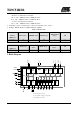
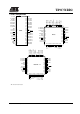
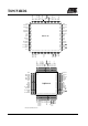
T89C51RD2
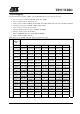
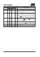
Mnemonic
Pin Number
Type
Name and Function
DIL LCC VQFP 1.4
V
SS
20 22 16 I Ground: 0V reference
Vss1 1 39 I Optional Ground: Contact the Sales Office for ground connection.
V
CC
40 44 38 I
Power Supply: This is the power supply voltage for normal, idle and power-
down operation
P0.0-P0.7 39-32 43-36 37-30 I/O Port 0: Port 0 is an open-drain, bidirectional I/O port. Port 0 pins that have 1s
written to them float and can be used as high impedance inputs. Port 0 must be
polarized to V
CC
or V
SS
in order to prevent any parasitic current consumption.
Port 0 is also the multiplexed low-order address and data bus during access to
external program and data memory. In this application, it uses strong internal
pull-up when emitting 1s. Port 0 also inputs the code bytes during EPROM
programming. External pull-ups are required during program verification during
which P0 outputs the code bytes.
P1.0-P1.7 1-8 2-9 40-44
1-3
I/O Port 1: Port 1 is an 8-bit bidirectional I/O port with internal pull-ups. Port 1 pins
that have 1s written to them are pulled high by the internal pull-ups and can be
used as inputs. As inputs, Port 1 pins that are externally pulled low will source
current because of the internal pull-ups. Port 1 also receives the low-order address
byte during memory programming and verification.
Alternate functions for TSC8x54/58 Port 1 include:
1 2 40 I/O T2 (P1.0): Timer/Counter 2 external count input/Clockout
2 3 41 I T2EX (P1.1): Timer/Counter 2 Reload/Capture/Direction Control
3 4 42 I ECI (P1.2): External Clock for the PCA
4 5 43 I/O CEX0 (P1.3): Capture/Compare External I/O for PCA module 0
5 6 44 I/O CEX1 (P1.4): Capture/Compare External I/O for PCA module 1
6 7 1 I/O CEX2 (P1.5): Capture/Compare External I/O for PCA module 2
7 8 2 I/O CEX3 (P1.6): Capture/Compare External I/O for PCA module 3
8 9 3 I/O CEX4 (P1.7): Capture/Compare External I/O for PCA module 4
P2.0-P2.7 21-28 24-31 18-25 I/O Port 2: Port 2 is an 8-bit bidirectional I/O port with internal pull-ups. Port 2
pins that have 1s written to them are pulled high by the internal pull-ups and
can be used as inputs. As inputs, Port 2 pins that are externally pulled low will
source current because of the internal pull-ups. Port 2 emits the high-order address
byte during fetches from external program memory and during accesses to external
data memory that use 16-bit addresses (MOVX @DPTR).In this application, it
uses strong internal pull-ups emitting 1s. During accesses to external data memory
that use 8-bit addresses (MOVX @Ri), port 2 emits the contents of the P2 SFR.
Some Port 2 pins receive the high order address bits during EPROM programming
and verification:
P2.0 to P2.5 for RB devices
P2.0 to P2.6 for RC devices
P2.0 to P2.7 for RD devices.
P3.0-P3.7 10-17 11,
13-19
5,
7-13
I/O Port 3: Port 3 is an 8-bit bidirectional I/O port with internal pull-ups. Port 3 pins
that have 1s written to them are pulled high by the internal pull-ups and can be
used as inputs. As inputs, Port 3 pins that are externally pulled low will source
current because of the internal pull-ups. Port 3 also serves the special features
of the 80C51 family, as listed below.
10 11 5 I RXD (P3.0): Serial input port
11 13 7 O TXD (P3.1): Serial output port
12 14 8 I INT0 (P3.2): External interrupt 0
13 15 9 I INT1 (P3.3): External interrupt 1
14 16 10 I T0 (P3.4): Timer 0 external input
15 17 11 I T1 (P3.5): Timer 1 external input
16 18 12 O WR (P3.6): External data memory write strobe