
Owner manual


8 Rev. F - 15 February, 2001
T89C51RD2
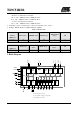
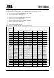
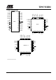
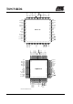
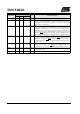
Mnemonic
Pin Number
Type
Name and Function
DIL LCC VQFP 1.4
17 19 13 O RD (P3.7): External data memory read strobe
Reset 9 10 4 I/O Reset: A high on this pin for two machine cycles while the oscillator is running,
resets the device. An internal diffused resistor to V
SS
permits a power-on reset
using only an external capacitor to V
CC
. This pin is an output when the hardware
watchdog forces a system reset.
ALE/PROG 30 33 27 O (I) Address Latch Enable/Program Pulse: Output pulse for latching the low byte
of the address during an access to external memory. In normal operation, ALE
is emitted at a constant rate of 1/6 (1/3 in X2 mode) the oscillator frequency,
and can be used for external timing or clocking. Note that one ALE pulse is
skipped during each access to external data memory. This pin is also the program
pulse input (PROG) during Flash programming. ALE can be disabled by setting
SFR’s AUXR.0 bit. With this bit set, ALE will be inactive during internal fetches.
PSEN 29 32 26 O Program Store ENable: The read strobe to external program memory. When
executing code from the external program memory, PSEN is activated twice each
machine cycle, except that two PSEN activations are skipped during each access
to external data memory. PSEN is not activated during fetches from internal
program memory.
EA 31 35 29 I External Access Enable: EA must be externally held low to enable the device
to fetch code from external program memory locations 0000H to FFFFH (RD).
If security level 1 is programmed, EA will be internally latched on Reset.
XTAL1 19 21 15 I
Crystal 1: Input to the inverting oscillator amplifier and input to the internal
clock generator circuits.
XTAL2 18 20 14 O Crystal 2: Output from the inverting oscillator amplifier