Features • Programmable DMUX Ratio: • • • • • • • • • • • • • • – 1:4: Data Rate Max = 1 Gsps – PD (8b/10b) < 4.3/4.7 W (ECL 50Ω output) – 1:8: Data Rate Max = 2 Gsps – PD (8b/10b) < 6/6.
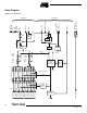
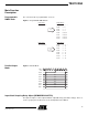
Block Diagram Figure 1. Block Diagram FS/8 ADCDelAdjIn ADCDelAdjCtrl RatioSel SyncReset AsyncReset ClkIn (to be confirmed) RatioSel NbBit ClkInType DEMUXDelAdjCtrl Clock Path I[0..7/9] BIST SwiAdj VplusDOut VCC GND VEE DIODE Data Path delay delay NAP B2 mux BIST 8/10 mux Phase control 8/10 RstGen ClkPar even master latch odd master latch odd slave latch Counter (8 stage shift register) 8 Counter Status Latch Sel Even/Odd [1..
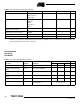
TS81102G0 Internal Timing Diagram This diagram corresponds to an established operation of the DMUX with Synchronous Reset. Figure 2.
Functional Description The TS81102G0 is a demultiplexer based on an advanced high-speed bipolar technology featuring a cutoff frequency of 25 GHz. Its role is to reduce the data rate so that the data can be processed at the DMUX output. The TS81102G0 provides 2 programmable ratios: 1:4 and 1:8. The maximum data rate is 1 Gsps for the 1:4 ratio and 2 Gsps for the 1:8 ratio. The TS81102G0 is able to process 8 or 10-bit data flows.
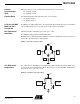
TS81102G0 Main Function Description Programmable DMUX Ratio The conversion ratio is programmable: 1:4 or 1:8. Figure 3. Programmable DMUX Ratio Input Words: Output Words: 1,2,3,4,5,6,7,8,... PortA PortB 1 5 2 6 PortC 3 7 8 1:4 PortD 4 PortE not used PortF not used PortG not used PortH not used Input Words: Output Words: 1,2,3,4,5,6,7,8,... PortA PortB 1 2 9 ... 10 PortC 3 11 PortD 4 12 PortE 5 13 PortF 6 14 PortG 7 15 PortH 8 16 1:8 Parallel Output Mode ...
Asynchronous Reset (ASYNCRESET) Figure 5. Asynchronous Reset CLKIN AsyncReset Port A selected Port B selected Port C selected Port D selected Port E selected Port F selected Port G selected Port H selected The Asynchronous Reset is a master reset of the port selection, which works on TTL levels. It is active on the high level. During an asynchronous reset, the clock must be in a known state. It is used to start the DMUX.
TS81102G0 Counter Programmable State When the counter is reset, its initial states depends on the conversion ratio: Pipeline Delay The maximum pipeline delay depends on the conversion ratio: • 1:8: counting on 8 bits, • 1:4: counting on 4 bits. • 1:8: pipeline delay = 7 • 1:4: pipeline delay = 3 8-/10-bit, with NAP Mode for the 2 Unused Bit The DMUX is a 10-bit parallel device.
Single-ended Output Data To reduce the pin number and power consumption of the DMUX, the eight output ports are single-ended. To reach the high frequency output (up to 250 MHz) with a reasonable power consumption, the swing must be limited to a maximum of ±500 mV. The common mode is adjustable from -1.3V to +2V, with Vplus DOut pins. To ensure better noise immunity, a reference level (common mode) is available (one level by output port).
TS81102G0 Differential Data Ready Output The front edge of the DataReady output occurs when data is available on the corresponding port. The frequency of this clock depends on the conversion ratio (1:8 or 1:4), with a duty cycle of 50%. The definition is the same as for single-ended output data, but the buffers are differential. This corresponds to the “Adjustable Logic Differential” in the pinout description. Built-in Self Test (BIST) A pseudo-random 10-bit generator is implemented in the DMUX.
Table 2.
TS81102G0 Electrical Operating Characteristics Tj (typical) = 70°C. Full Temperature Range: -40°C < Tc; Tj < 110°C. (Guaranteed temperature range are depending on part number) Table 4. Electrical Specifications Parameter Symbol Test Level Value Min Typ Max Unit 5 – 0 3.3 3.3 5.25 – 0.25 3.465 3.465 V – V V V -5 -4.75 V Note Power Requirements Positive supply voltage VCC VPLUSDOUT ECL PECL TTL VCC – VPLUSD VPLUSD VPLUSD 1 4.75 – -0.25 3.135 3.135 VEE 1 -5.
Table 4. Electrical Specifications (Continued) Parameter Symbol PECL (50Ω) 1:8, 8 bits 1:8, 10 bits 1:4, 8 bits 1:4, 10 bits PD PD PD PD TTL (75Ω) 1:8, 8 bits 1:8, 10 bits 1:4, 8 bits 1:4, 10 bits PD PD PD PD Test Level Value Min Typ Max Unit 1 5.8 6.6 4.2 4.6 6.2 7.1 4.4 4.8 6.6 7.6 4.6 5.1 W W W W 1 6.8 7.8 4.7 5.2 7.3 8.4 4.9 5.5 7.7 9 5.1 5.8 W W W W – – – – – – – -0.5 0 0.5 – – – – – – V V V mA – – – – – – – -0.5 0 0.
TS81102G0 Table 4. Electrical Specifications (Continued) Parameter Output level drift with temperature (reference outputs) Value Symbol Test Level Min Typ Max Unit – 1 – -0.9 – mV/°C VIL VIH 1 – -1.1 – – -1.4 – V V Note Digital Inputs ECL Input Voltages Logic “0” voltage Logic “1” voltage TTL Input Voltages – – 0.8 Logic “0” voltage VIL 1 VIH 2.0 – – Logic “1” voltage Note: 1.
Table 5.
TS81102G0 Table 5. Switching Performances (Continued) Value Parameter Symbol Test Level Setup time from Bist to Clkln TSBIST – – 1000 – ps Rise/fall time for (10% – 90%) TRBIST/ TFBIST – 1000 – – ps Input frequency FMADA – 2 – 2.
Input Clock Timings Figure 10. Input Clock TC2 TC2 TFCKIN TFCKIN TC1 TC1 TRCKIN TRCKIN Clkln TSCKIN Data [0..9] d1 d2 TSCKIN THCKIN d3 d4 d5 d1 Clkln Type = 1 DataReady Mode (DR) d2 THCKIN d3 d4 d5 Clkln Type = 0 DataReady/2 Mode (DR/2) ADC Delay Adjust Timing Diagram Figure 11.
TS81102G0 Timing Diagrams with Asynchronous Reset With a nominal tuning of DMUXDelAdj at a frequency of 2 GHz, d1 and d2 data is lost because of the internal clock’s path propagation delay TCPD. TCPD is tuned with DMUXDelAdjCtrl pins to obtain good setup and hold times between Clkln and the data. Figure 12. Start with Asynchronous Rest, 1:8 Ratio, DR Mode TRAR TFAR PWAR ASyncReset TPD Clkn TCPD Internal Port Selection (not available out of the DEMUX) A I[0..
With a nominal tuning of DMUXDelAdj, at 1 GHz (1:4 mode) d1 data is lost because of the internal clock’s path propagation delay TCPD. TCPD is tuned with DMUXDelAdjCtrl pins and is used to obtain good setup and hold times between Clkln and the input data. Figure 14. Start with Asynchronous Reset, 1:4 Ratio, DR Mode TRAR TFAR PWAR ASyncReset TPD Clkn TCPD Internal Port Selection (not available out of the DEMUX) A I[0..9] d1 B d2 C D d3 A d4 B d5 C d6 D d7 d8 TOD TOD d5 A[0..9] B[0..
TS81102G0 Timing Diagrams with Synchronous Reset Following is an example of the Synchronous Reset’s utility in case of de-synchronization of the DMUX output port selection. The de-synchronization event happens after the selection of Port D. DMUXDelAdjCtrl value is nominal. TSSR < 0 because of Clkln’s internal propagation delay TCPD. After selection of Port C, instead of selecting Port D, the de-synchronization makes the port selection to restart on Port A.
Figure 17. Synchronous Reset, 1:4 Ratio, DR Mode THSR SyncReset TSSR Clkn TCPD I[0..9] d1 d2 Internal Port Selection (not available out of the DEMUX) d3 B C d4 d5 D A d6 d7 B C d8 d9 D d10 A B d11 d12 C D d13 d14 A B d16 d15 C D TOD A[0..9] d1 d9 B[0..9] d2 d10 C[0..9] d3 d11 D[0..9] d4 d12 TDRF TDRR DR Period of uncertainty due to desynchronization Example of Synchronous Reset’s utility in case of de-synchronization of the DMUX output port selection.
TS81102G0 Figure 19. Synchronous Reset, 1:4 ratio, DR/2 Mode THSR SyncReset TSSR Clkn I[0..9] d1 d2 d3 d4 d5 d6 d7 d8 d9 d10 d12 d11 d13 d14 d15 d16 TCPD Internal Port Selection (not available out of the DEMUX) B C D A B C A A B C D A B C D TOD A[0..9] d1 B[0..9] d2 C[0..9] d3 D[0..
Explanation of Test Levels Table 6. Explanation of Test Levels Num 1 100% production tested at +25°C.(1) 2 100% production tested at +25°C, and sample tested at specified temperatures.(1) 3 Sample tested only at specified temperatures. 4 Parameter is guaranteed by design and characterization testing (thermal steady-state conditions at specified temperature). 5 Parameter is a typical value only. Notes: 22 Characteristics 1. The level 1 and 2 tests are performed at 50 MHz. 2.
TS81102G0 Package Description Pin Description Table 7. TS81102G0 Pin Description Type Name Levels Comments Digital Inputs I[0…9] Differential ECL Data input. On-chip 100Ω differential termination resistor. Clkln Differential ECL Clock input (Data Ready ADC). On-chip 100Ω differential termination resistor. A[0…9] → H[0…9] Adjustable Logic Single Data ready for port A to H. Common mode is adjusted with VplusDOut. Swing is adjusted with SwiAdj. 50Ω termination possible.
TBGA 240 Package – Pinout Row A A A A A A A A A A A A A A A A A A A B B B B B B B B B B B B B B B B B B B C C C C C C C C C C C C C C C C C C C D D D 24 Col 1 2 3 4 5 6 7 8 9 10 11 12 13 14 15 16 17 18 19 1 2 3 4 5 6 7 8 9 10 11 12 13 14 15 16 17 18 19 1 2 3 4 5 6 7 8 9 10 11 12 13 14 15 16 17 18 19 1 2 3 Name NC E3 E5 E7 E9 C0 C2 C4 C6 C8 REFA A1 A3 A5 A7 A9 DEMUXDELADJCTRL RSTSYNCB NC E1 E2 E4 E6 E8 REFC C1 C3 C5 C7 C9 A0 A2 A4 A6 A8 ASYNCRESET DEMUXDELADJCTRLB RSTSYNC REFE E0 VEE VPLUSDOUT VPLUSDOUT V
TS81102G0 Figure 20.
Outline Dimensions Figure 21. Package Dimension – 240 Tape Ball Grid Array 11 0.10 D 10 -A- Corner 19 17 15 13 11 9 7 5 3 1 -B- Ref. A A1 D D1 E E1 b c M N aaa ccc e g P 18 16 14 12 10 8 6 4 2 A B C D E F G H J K L M N P R T U V W e E E1 e 45 degree 0.5 mm chamfer (4 PLCS) Detail B D1 Top View Bottom View Dimensional References Min. Nom. 1.30 1.50 0.50 0.60 24.80 25.00 22.86 (BSC.) 24.80 25.00 22.86 (BSC.) 0.60 0.75 0.90 0.80 19.00 240.00 1.27 TYP. 0.35 0.15 Max. 1.70 0.70 25.20 25.20 0.
TS81102G0 Thermal Resistance from Junction to Ambient: RTHJA A pin-fin type heat sink of a size 40 mm x 40 mm x 8 mm can be used to reduce thermal resistance. This heat sink should not be glued to the top of the package as Atmel cannot guarantee the attachment to the board in such a configuration. The heat sink could be clipped or screwed on the board.
Temperature Diode Characteristic The theoretical characteristic of the diode according to the temperature when I = 3 mA is depicted below. Figure 23. Temperature Diode Characteristic Vdiode DiodeT 1.0 I = 3 mA dV/dT = 1.32 mV/°C (V) 900m 800m 700m -70.0 -20.0 30.0 80.0 130.0 Temperature (°C) Moisture Characteristic This device is sensitive to moisture (MSL3 according to the JEDEC standard). The shelf life in a sealed bag is 12 months at < 40°C and < 90% relative humidity (RH).
TS81102G0 Detailled Cross Section The following diagram depicts a detailed cross section of the DMUX TBGA package. Figure 24.
Applying the TS81102G0 DMUX The TSEV81102G0 DMUX evaluation board is designed to be connected with the TSEV8388G and TSEV83102G0 ADC evaluation boards. Figure 25. TSEV81102G0 DMUX Evaluation Boards VplusD = 0V → 3.3V CLOCK BUFFER s-e or diff. (2 GHz) Vee = -5V FS Vcc = +5V (125 MHz) 8x8b/10b single A[0..9] → H[0..9] DEMUX Analog Input ADC (1 GHz) 8b/10b diff. Data Bus RefA → RefH (250 MHz) 1b diff. I[0..9] (1 - 2 GHz) 1b diff.
TS81102G0 ADC to DMUX Connections The DMUX inputs configuration has been optimized to be connected to the TS8388B ADC. The die in the TBGA package is up. For the ADC, different types of packages can be used such as CBGA with die up or the CQFP68 down. The DMUX device being completely symmetrical, both ADC packages can be connected to the TBGA package of the DMUX crisscrossing the lines (see Table 8). Table 8.
TSEV81102G0TP: Device Evaluation Board General Description The TSEV81102G0TP DMUX Evaluation Board (EB) is designed to simplify the characterization and the evaluation of the TS81102G0 device (2 Gsps DMUX).
TS81102G0 Ordering Information Table 9. Ordering Information Part Number Package JTS81102G0-1V1A Die TS81102G0CTP TBGA 240 "C" grade 0°C < Tc; Tj < 90°C Standard TS81102G0VTP TBGA 240 "V" grade -40°C < Tc; Tj < 110°C Standard TSEV81102G0TPZR3 TBGA 240 Ambient Prototype Datasheet Status Description Temperature Range Ambient Screening Comments Visual inspection Evaluation board (delivered with heatsink) Table 10.
Addendum This section has been added to the description of the device for better understanding of the synchronous reset operation. It puts particular stress on the setup and hold times defined in the switching characteristics table (Table 5), linked with the device performances when used at full speed (2 Gsps). Synchronous Reset Operation It first describes the operation of the synchronous reset in case the DMUX is used in DR mode and then when used in the DR/2 mode.
TS81102G0 Figure 27. Synchronous Reset Operation in DR Mode, 1:4 ratio, 1GHz (Full Speed) – TIMINGS Fs Time Zones Allowed for the reset Sync_RESET Note: The clock edge to which the reset applies is the one identified by the arrow. If the reset rising edge had occurred in the second allowed window, the reset would have been effective on the third clock rising edge (not represented, on the right of the edge represented with the arrow). Figure 28.
Operation in DR/2 Mode In DR/2 mode, the DMUX input clock can run at up to 1 GHz in 1:8 ratio or 500 MHz in 1:4 ratio, since the DR/2 clock from the ADC is half the sampling frequency. Both cases are described in the following timing diagrams. Figure 30. Synchronous Reset Operation in DR/2 Mode, 1:4 ratio, 500MHz (Full Speed) – Principle of Operation Fs/2 Sync_RESET Figure 31.
TS81102G0 Figure 33. Synchronous Reset Operation in DR/2 Mode, 1:8 ratio, 1GHz (Full-speed) – Timings Fs/2 Times Zones Allowed for the reset Sync_RESET Note: The clock edge to which the reset applies is the one identified by the arrow. If the reset rising edge had occurred in the second allowed window, the reset would have been effective on the fourth clock rising edge (not represented, on the right of the edge represented with the arrow).
Atmel Headquarters Atmel Operations Corporate Headquarters Memory 2325 Orchard Parkway San Jose, CA 95131, USA TEL 1(408) 441-0311 FAX 1(408) 487-2600 Europe Atmel Sarl Route des Arsenaux 41 Case Postale 80 CH-1705 Fribourg Switzerland TEL (41) 26-426-5555 FAX (41) 26-426-5500 Asia Room 1219 Chinachem Golden Plaza 77 Mody Road Tsimhatsui East Kowloon Hong Kong TEL (852) 2721-9778 FAX (852) 2722-1369 Japan 9F, Tonetsu Shinkawa Bldg.