
User guide

TSM10N06
60V N-Channel MOSFET
1/6
Version: A10
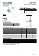
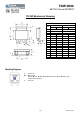
TO
-
252
(DPAK)
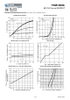
PRODUCT SUMMARY
V
DS
(V) R
DSON
(mΩ) I
D
(A)
60
65 @ V
GS
= 10V 10
80 @ V
GS
= 5V 10
110 @ V
GS
= 4V 9
Features
● Advance Trench Process Technology
● High Density Cell Design for Ultra Low On-resistance
Application
● Load Switch
● PA Switch
Ordering Information
Part No. Package
Packing
TSM10N06CP RO
TO-252 2.5Kpcs / 13” Reel
Absolute Maximum Rating
(T
A
= 25
o
C unless otherwise noted)
Parameter Symbol Limit Unit
Drain-Source Voltage V
DS
60 V
Gate-Source Voltage V
GS
±20 V
Continuous Drain Current I
D
10 A
Pulsed Drain Current I
DM
50 A
Continuous Source Current (Diode Conduction)
a,b
I
S
10 A
Total Power Dissipation @ T
C
=25C P
DTOT
45 W
Operating Junction Temperature T
J
+150
o
C
Operating Junction and Storage Temperature Range T
J
, T
STG
- 55 to +150
o
C
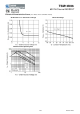
Thermal Performance
Parameter Symbol Limit Unit
Junction to Case Thermal Resistance RӨ
JC
2.78
o
C/W
Junction to Ambient Thermal Resistance (PCB mounted) RӨ
JA
50
o
C/W
Notes:
a. Pulse width limited by the Maximum junction temperature
b. Surface Mounted on FR4 Board, t ≤ 10 sec.
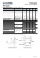
Block Diagram
N-Channel MOSFET
Pin
Definition
:
1. Gate
2. Drain
3. Source