
User Manual

TSM13N50
500V N-Channel Power MOSFET
1/10
Version: C12
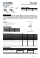
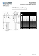
TO
-
220
ITO
-
220
PRODUCT SUMMARY
V
DS
(V) R
DS(on)
(Ω) I
D
(A)
500 0.48 @ V
GS
=10V 13
General Description
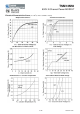
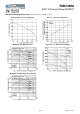
The TSM13N50 N-Channel enhancement mode Power MOSFET is produced by planar stripe DMOS technology.
This advanced technology has been especially tailored to minimize on-state resistance, provide superior switching
performance, and withstand high energy pulse in the avalanche and commutation mode. These devices are well
suited for high efficiency switch mode power supply, power factor correction, electronic lamp ballast based on half
bridge.
Features
● Low R
DS(ON)
0.38Ω (Typ.)
● Low gate charge typical @ 36nC (Typ.)
● Low Crss typical @ 7.7pF (Typ.)
● Fast Switching
Ordering Information
Part No. Package Packing
TSM13N50CZ C0
TO-220 50pcs / Tube
TSM13N50CI C0 ITO-220 50pcs / Tube
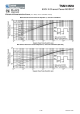
Absolute Maximum Rating
(Ta = 25
o
C unless otherwise noted)
Parameter Symbol Limit Unit
Drain-Source Voltage V
DS
500 V
Gate-Source Voltage V
GS
±30 V
Continuous Drain Current(T
C
=25 )℃ I
D
13 A
Pulsed Drain Current * I
DM
52 A
Peak Diode Recovery dv/dt (Note 3) dv/dt 4.5 V/ns
Single Pulse Avalanche Energy (Note 2) E
AS
563 mJ
Avalanche Current (Repetitive) (Note 1) I
AR
13 A
Repetitive Avalanche Energy (Note 1) E
AR
18.3 mJ
Operating Junction Temperature T
J
150 ºC
Storage Temperature Range T
STG
-55 to +150
o
C
* Limited by maximum junction temperature
Thermal Performance
Parameter Symbol Limit Unit
Thermal Resistance - Junction to Case
TO-220
RӨ
JC
0.63
o
C/W ITO-220 2.4
Thermal Resistance - Junction to Ambient TO-220 / ITO-220
RӨ
JA
62.5
Notes: Surface mounted on FR4 board t ≤ 10sec
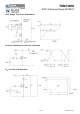
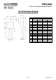
Block Diagram
N-Channel MOSFET
Pin
Definition
:
1. Gate
2. Drain
3. Source