
Manual

TSM15N03PQ33
30V N-Channel Power MOSFET
1/4
Version: A12
PDFN
33
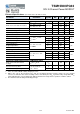
PRODUCT SUMMARY
V
DS
(V) R
DS(on)
(mΩ) I
D
(A)
30
12 @ V
GS
=10V 7.8
17 @ V
GS
=4.5V 7
Features
● Advanced Trench Technology
● Low On-Resistance
● Low gate charge typical @ 3.6nC (Typ.)
● Low Crss typical @ 38pF (Typ.)
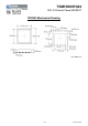
Block Diagram
N-Channel MOSFET
Ordering Information
Part No. Package
Packing
TSM15N03PQ33 RGG PDFN33 5Kpcs / 13” Reel
Note: “G” denote for Halogen Free Product
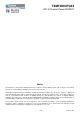
Absolute Maximum Rating
(Ta = 25
o
C unless otherwise noted)
Parameter Symbol Limit Unit
Drain-Source Voltage V
DS
30 V
Gate-Source Voltage V
GS
±20 V
Continuous Drain Current
T
C
=25°C
I
D
14
A
T
C
=70°C 14
T
A
=25°C 9.7
T
A
=70°C 7.8
Drain Current-Pulsed Note 1 I
DM
35 A
Avalanche Current, L=0.1mH I
AS
, I
AR
9 A
Avalanche Energy, L=0.1mH E
AS
, E
AR
4 mJ
Maximum Power Dissipation
T
C
=25°C
P
D
15.6
W
T
C
=70°C 10
T
A
=25°C 3.2
T
A
=70°C 2.1
Storage Temperature Range T
STG
-55 to +150 °C
Operating Junction Temperature Range T
J
-55 to +150 °C
* Limited by maximum junction temperature
Thermal Performance
Parameter Symbol Limit Unit
Thermal Resistance - Junction to Case RӨ
JC
8
o
C/W
Thermal Resistance - Junction to Ambient RӨ
JA
40
o
C/W
Notes: Surface mounted on FR4 board t ≤ 10sec
Pin
Definition
:
1. Source 8. Drain
2. Source 7. Drain
3. Source 6. Drain
4. Gate 5. Drain