
Instruction Manual

TSM160N10
100V N-Channel Power MOSFET
1/6
Version: B13
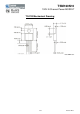
TO
-
220
PRODUCT SUMMARY
V
DS
(V) R
DS(on)
(mΩ) I
D
(A)
100 5.5 @ V
GS
=10V 160
Features
● Advanced Trench Technology
● Low R
DS(ON)
5.5mΩ (Max.)
● Low gate charge typical @ 154nC (Typ.)
● Low Crss typical @ 300pF (Typ.)
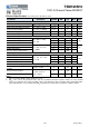
Block Diagram
N-Channel MOSFET
Ordering Information
Part No. Package Packing
TSM160N10CZ C0 TO-220 50pcs / Tube
Absolute Maximum Rating
(Ta = 25
o
C unless otherwise noted)
Parameter Symbol Limit Unit
Drain-Source Voltage V
DS
100 V
Gate-Source Voltage V
GS
±20 V
Continuous Drain Current
T
C
=25°C
I
D
160
A
T
C
=70°C 127
T
A
=25°C 14.2
T
A
=70°C 11.4
Drain Current-Pulsed Note 1 I
DM
620 A
Avalanche Current, L=0.5mH I
AS
, I
AR
40 A
Avalanche Energy, L=0.5mH E
AS
, E
AR
400 mJ
Maximum Power Dissipation
T
C
=25°C
P
D
300
W
T
C
=70°C 210
T
A
=25°C 2.4
T
A
=70°C 1.68
Storage Temperature Range T
STG
-55 to +175 °C
Operating Junction Temperature Range T
J
-55 to +175 °C
* Limited by maximum junction temperature
Thermal Performance
Parameter Symbol Limit Unit
Thermal Resistance - Junction to Case RӨ
JC
0.5
o
C/W
Thermal Resistance - Junction to Ambient RӨ
JA
62.5
o
C/W
Notes: Surface mounted on FR4 board t ≤ 10sec
Pin
Definition
:
1. Gate
2. Drain
3. Source