
User guide
TSM1N45
450V N-Channel Power MOSFET
1/9
Version: C09
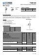
TO
-
92
SOT
-
223
General Description
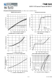
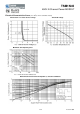
The TSM1N45 is N-Channel enhancement mode power field effect transistors are produced using planar DMOS
technology process. This advanced technology has been especially tailored to minimize on-state resistance,
provide superior switching performance, and withstand higher energy pulse in the avalanche and commutation
mode. There devices are well suited for electronic ballasts base and half bridge configuration.
Features
● Low gate charge @ typical 6.5nC
● Low Crss @ typical 6.5pF
● Avalanche energy specified
● Improved dv/dt capability
● Gate-Source Voltage ±30V guaranteed
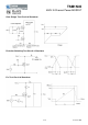
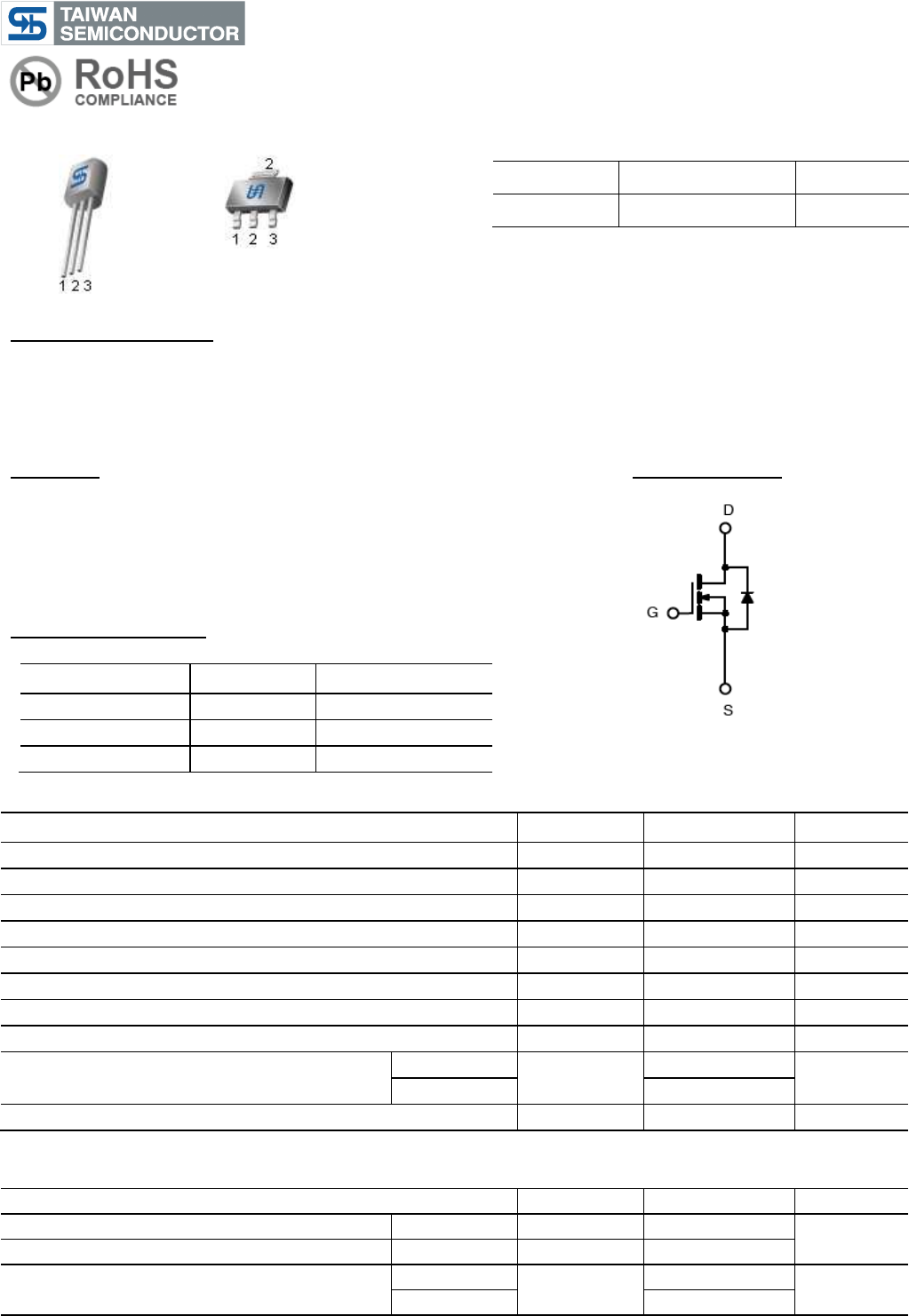
Block Diagram
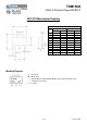
Ordering Information
Part No. Package Packing
TSM1N45CT B0 TO-92 1Kpcs / Bulk
TSM1N45CT A3 TO-92 2Kpcs / Ammo
TSM1N45CW RP SOT-223 2.5Kpcs / 13” Reel
Absolute Maximum Rating
(Ta=25
o
C unless otherwise noted)
Parameter Symbol Limit Unit
Drain-Source Voltage
V
DS
450 V
Gate-Source Voltage
V
GS
±30 V
Continuous Drain Current
I
D
0.5 A
Pulsed Drain Current (Note 1)
I
DM
4 A
Single Pulse Drain to Source Avalanche Energy (Note 2) E
AS
108 mJ
Avalanche Current (Note 1)
I
A
R
0.5 A
Repetitive Avalanche Energy (Note 1)
E
A
R
0.25 mJ
Peak Diode Recovery dv/dt (Note 3)
dv/dt 5.5 V/ns
Total Power Dissipation @T
C
=25ºC
TO-92
P
DTOT
2
W
SOT-223
15
Operating Junction and Storage Temperature Range
T
J
, T
STG
-55 to +150
o
C
*Surface Mounted on 1”x1” FR4 board
Thermal Performance
Parameter Symbol Limit Unit
Thermal Resistance - Junction to Lead TO-92 RӨ
JL
50
o
C/W
Thermal Resistance - Junction to Case SOT-223 RӨ
JC
8.5
Thermal Resistance - Junction to Ambient *
TO-92
RӨ
JA
140
o
C/W
SOT-223 60
*When mounted on the minimum pad size recommended (PCB mount)
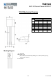
Pin
Definition
:
1. Gate
2. Drain
3. Source
N-Channel MOSFET
PRODUCT SUMMARY
V
DS
(V) R
DS(on)
(Ω) I
D
(A)
450 4.25 @ V
GS
=10V 0.25