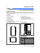
Preliminary W24256 32K × 8 CMOS STATIC RAM GENERAL DESCRIPTION The W24256 is a normal speed, very low power CMOS static RAM organized as 32768 × 8 bits that operates on a single 5-volt power supply. This device is manufactured using Winbond's high performance CMOS technology. FEATURES • Low power consumption: Access time: 70 nS (max.
Preliminary W24256 TRUTH TABLE MODE VDD CURRENT I/O1−I/O8 CS OE WE H X X Not Selected High Z ISB, ISB1 L H H Output Disable High Z IDD L L H Read Data Out IDD L X L Write Data In IDD DC CHARACTERISTICS Absolute Maximum Ratings PARAMETER Supply Voltage to VSS RATING Potential UNIT -0.5 to +7.0 V Input/Output to VSS Potential -0.5 to VDD +0.5 V Allowable Power Dissipation 1.
Preliminary W24256 CAPACITANCE (VDD = 5V, TA = 25° C, f = 1 MHz) PARAMETER SYM. CONDITIONS MAX. UNIT Input Capacitance CIN VIN = 0V 6 pF Input/Output Capacitance CI/O VOUT 8 pF = 0V Note: These parameters are sampled but not 100% tested. AC CHARACTERISTICS AC Test Conditions PARAMETER CONDITIONS Input Pulse Levels 0V to 3.0V Input Rise and Fall Times 5 nS Input and Output Timing Reference Level 1.
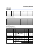
Preliminary W24256 AC Characteristics, continued (VDD = 5V ±10%; VSS = 0V; TA = 0° C to 70° C) Read Cycle PARAMETER SYM. W24256-70L/LL MIN. MAX.
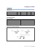
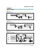
Preliminary W24256 TIMING WAVEFORMS Read Cycle 1 (Address Controlled) TRC Address TAA TOH TOH DOUT Read Cycle 2 (Chip Select Controlled) CS TACS TCHZ TCLZ DOUT Read Cycle 3 (Output Enable Controlled) T RC Address T AA OE T OH T AOE T OLZ CS T ACS D OUT T CHZ T OHZ TCLZ -5- Publication Release Date: October 1999 Revision A1
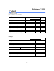
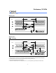
Preliminary W24256 Timing Waveforms, continued Write Cycle 1 TWC Address T WR OE TCW CS T AW WE T WP TAS TOHZ (1, 4) D OUT T DW TDH D IN Write Cycle 2 ( OE = VIL Fixed) T WC Address TWR TCW CS TAW WE TOH T WP TAS TWHZ (1, 4) D OUT TDW (2) (3) TOW TDH DIN Notes: 1. During this period, I/O pins are in the output state, so input signals of opposite phase to the outputs should not be applied. 2. The data output from DOUT are the same as the data written to DIN during the write cycle. 3.
Preliminary W24256 DATA RETENTION CHARACTERISTICS (TA = 0° C to 70° C) PARAMETER SYM. TEST CONDITIONS MIN. TYP. MAX. UNIT 2.0 - 5.5 V VDD for Data Retention VDR CS ≥ VDD -0.2V Data Retention Current IDDDR CS ≥ VDD -0.2V, VDD = 3V - - 20 µA Chip Deselect to Data Retention Time TCDR See data retention waveform 0 - - nS Operation Recovery Time TR TRC* - - nS * Read Cycle Time DATA RETENTION WAVEFORM VDD 0.9 V DD VDR > = 2V 0.9 V DD TCDR TR CS > = V DD - 0.
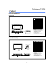
Preliminary W24256 PACKAGE DIMENSIONS 28-pin P-DIP Dimension in Inches Symbol A A1 A2 B B1 c D E E1 e1 L D 28 15 a E1 eA S Notes: 1 14 E S c A A2 A1 L Base Plane Seating Plane B e1 eA a B1 Min. Nom. Max. Dimension in mm Min. Nom. Max. 0.210 0.010 5.33 0.25 0.150 0.155 0.160 3.81 3.94 4.06 0.016 0.018 0.022 0.41 0.46 0.56 0.058 0.060 0.064 1.47 1.52 0.008 0.010 0.014 0.20 1.460 1.470 0.590 0.600 0.610 0.540 0.545 0.550 0.090 0.100 0.130 0.120 0 0.
Preliminary W24256 Package Dimensions, continued 28-pin Standard Type One TSOP HD Dimension In Inches Dimension In mm Symbol Min. D c A A1 A2 b c D E HD e L L1 Y θ 1 e E b A2 A θ A1 L Nom. Max. Min. Nom. 0.002 Max. 1.20 0.047 0.006 0.05 0.15 0.035 0.040 0.041 0.95 1.00 0.007 0.008 0.011 0.17 0.20 0.27 0.004 0.006 0.008 0.10 0.15 0.21 11.90 1.05 0.461 0.465 0.469 11.70 11.80 0.311 0.315 0.319 7.90 8.00 8.10 0.520 0.528 0.536 13.20 13.40 13.60 0.
Preliminary W24256 VERSION HISTORY VERSION DATE PAGE A1 Oct. 1999 - Headquarters DESCRIPTION Initial issued Winbond Electronics (H.K.) Ltd. Rm. 803, World Trade Square, Tower II, No. 4, Creation Rd. III, 123 Hoi Bun Rd., Kwun Tong, Science-Based Industrial Park, Kowloon, Hong Kong Hsinchu, Taiwan TEL: 852-27513100 TEL: 886-3-5770066 FAX: 852-27552064 FAX: 886-3-5796096 http://www.winbond.com.tw/ Voice & Fax-on-demand: 886-2-27197006 Taipei Office 11F, No. 115, Sec. 3, Min-Sheng East Rd.