W29EE011 128K × 8 CMOS FLASH MEMORY GENERAL DESCRIPTION The W29EE011 is a 1-megabit, 5-volt only CMOS flash memory organized as 128K × 8 bits. The device can be programmed and erased in-system with a standard 5V power supply. A 12-volt VPP is not required. The unique cell architecture of the W29EE011 results in fast program/erase operations with extremely low current consumption (compared to other comparable 5-volt flash memory products).
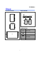
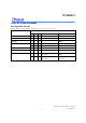
W29EE011 PIN CONFIGURATIONS BLOCK DIAGRAM NC 1 32 VDD A16 2 31 WE A15 3 30 NC A12 4 29 A14 A7 5 28 A13 A6 6 27 A8 A5 7 26 A9 A4 8 25 A11 OE A10 32-pin DIP A3 9 24 A2 10 23 A1 11 22 CE A0 12 21 DQ7 DQ0 13 20 DQ6 DQ1 14 19 DQ5 DQ2 15 18 DQ4 GND 16 17 DQ3 VDD VSS CE OE CONTROL WE . DECODER .
W29EE011 FUNCTIONAL DESCRIPTION Read Mode The read operation of the W29EE011 is controlled by CE and OE, both of which have to be low for the host to obtain data from the outputs. CE is used for device selection. When CE is high, the chip is de-selected and only standby power will be consumed. OE is the output control and is used to gate data from the output pins. The data bus is in high impedance state when either CE or OE is high. Refer to the timing waveforms for further details.
W29EE011 Hardware Data Protection The integrity of the data stored in the W29EE011 is also hardware protected in the following ways: (1) Noise/Glitch Protection: A WE pulse of less than 15 nS in duration will not initiate a write cycle. (2) VDD Power Up/Down Detection: The programming operation is inhibited when VDD is less than 3.8V. (3) Write Inhibit Mode: Forcing OE low, CE high, or WE high will inhibit the write operation. This prevents inadvertent writes during power-up or power-down periods.
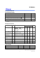
W29EE011 TABLE OF OPERATING MODES Operating Mode Selection Operating Range = 0 to 70°C (Ambient Temperature), VDD = 5V ±10%, VSS = 0V, VHH = 12V MODE PINS ADDRESS DQ.
W29EE011 Command Codes for Software Data Protection BYTE SEQUENCE TO ENABLE PROTECTION TO DISABLE PROTECTION ADDRESS DATA ADDRESS DATA 0 Write 5555H AAH 5555H AAH 1 Write 2AAAH 55H 2AAAH 55H 2 Write 5555H A0H 5555H 80H 3 Write - - 5555H AAH 4 Write - - 2AAAH 55H 5 Write - - 5555H 20H Sofware Data Protection Acquisition Flow Software Data Protection Enable Flow (Optional page load operation) Software Data Protection Disable Flow Load data AA to address 5555 Load data
W29EE011 Command Codes for Software Chip Erase BYTE SEQUENCE ADDRESS DATA 0 Write 5555H AAH 1 Write 2AAAH 55H 2 Write 5555H 80H 3 Write 5555H AAH 4 Write 2AAAH 55H 5 Write 5555H 10H Sofware Chip Erase Acquisition Flow Load data AA to address 5555 Load data 55 to address 2AAA Load data 80 to address 5555 Load data AA to address 5555 Load data 55 to address 2AAA Load data 10 to address 5555 Pause 50 mS Exit Notes for software chip erase: Data Format: DQ7−DQ0 (Hex) Address Format: A
W29EE011 Command Codes for Product Identification BYTE SEQUENCE 0 1 2 3 4 5 Write Write Write Write Write Write SOFTWARE PRODUCT IDENTIFICATION ENTRY ADDRESS DATA 5555H AAH 2AAAH 55H 5555H 80H 5555H AAH 2AAAH 55H 5555H 60H SOFTWARE PRODUCT IDENTIFICATION EXIT ADDRESS DATA 5555H AAH 2AAAH 55H 5555H F0H - Pause 10 µS Pause 10 µS Software Product Identification Acquisition Flow Product Identification Entry(1) Product Identification Mode(2, 3) Product Identification Exit(1) Load data AA to address 555
W29EE011 DC CHARACTERISTICS Absolute Maximum Ratings PARAMETER RATING UNIT Power Supply Voltage to Vss Potential Operating Temperature -0.5 to +7.0 0 to +70 V °C Storage Temperature -65 to +150 °C D.C. Voltage on Any Pin to Ground Potential except OE -0.5 to VDD +1.0 V Transient Voltage (< 20 nS ) on Any Pin to Ground Potential -1.0 to VDD +1.0 -0.5 to 12.
W29EE011 CAPACITANCE (VDD = 5.0V, TA = 25° C, f = 1 MHz) PARAMETER SYMBOL CONDITIONS MAX. UNIT I/O Pin Capacitance CI/O VI/O = 0V 12 pF Input Capacitance CIN VIN = 0V 6 pF AC CHARACTERISTICS AC Test Conditions (VDD = 5V ±10%) PARAMETER CONDITIONS Input Pulse Levels Input Rise/Fall Time 0V to 3V < 5 nS Input/Output Timing Level 1.5V/1.5V Output Load 1 TTL Gate and CL = 30 pF for 70 nS and 100 pF for others. AC Test Load and Waveforms +5V 1.
W29EE011 Read Cycle Timing Parameters (VCC = 5.0V ±10%, VCC = 5.0 ±5% for 70 nS, VSS = 0V, TA = 0 to 70° C) PARAMETER W29EE011-90 SYM. W29EE011-15 MIN. MAX. MIN. MAX.
W29EE011 Data Polling and Toggle Bit Timing Parameters PARAMETER W29EE011-90 SYM. W29EE011-15 UNIT MIN. MAX. MIN. MAX.
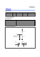
W29EE011 Timing Waveforms, continued WE Controlled Write Cycle Timing Diagram TBLCO TAS T WC TAH Address A16-0 TCS CE TCH TOES T OEH OE TWP WE TWPH TDS DQ7-0 Data Valid TDH Internal write starts CE Controlled Write Cycle Timing Diagram TAS TBLCO T AH TWC Address A16-0 TCPH T CP CE T OES T OEH OE WE T DS DQ7-0 High Z Data Valid T DH Internal Write Starts - 13 - Publication Release Date: July 1999 Revision A12
W29EE011 Timing Waveforms, continued Page Write Cycle Timing Diagram TWC Address A16-0 DQ7-0 CE OE T WPH TBLCO TBLC TWP WE Byte 0 Byte 1 Byte 2 Byte N-1 Byte N Internal Write Start DATA Polling Timing Diagram Address A16-0 WE TCEP CE TOES TOEH OE TOEP DQ7-0 X X X T WC - 14 - X
W29EE011 Timing Waveforms, continued Toggle Bit Timing Diagram Address A16-0 WE CE TOES TOEH OE DQ6 TWC Page Write Timing Diagram Software Data Protection Mode Address A16-0 2AAA 5555 DQ6 AA TWC Byte/page load cycle starts Three-byte sequence for software data protection mode 5555 55 A0 CE OE TBLC TWP WE TBLCO TWPH SW0 SW1 SW2 Byte 0 Byte N-1 Byte N (last byte) Internal write starts - 15 - Publication Release Date: July 1999 Revision A12
W29EE011 Timing Waveforms, continued Reset Software Data Protection Timing Diagram Six-byte sequence for resetting software data protection mode Address A16-0 5555 2AAA 5555 DQ7-0 AA 55 80 5555 AA TWC 2AAA 5555 55 20 CE OE TWP TBLC TBLCO WE TWPH SW0 SW2 SW1 SW3 SW4 SW5 Internal programming starts 5 Volt-only Software Chip Erase Timing Diagram Six-byte code for 5V-only software chip erase Address A16-0 5555 2AAA 5555 DQ7-0 AA 55 80 5555 AA TWC 2AAA 5555 55 10 CE O
W29EE011 ORDERING INFORMATION ACCESS TIME (nS) POWER SUPPLY CURRENT MAX. (mA) STANDBY VDD CURRENT MAX.
W29EE011 PACKAGE DIMENSIONS 32-pin P-DIP Symbol A A1 A2 B B1 c D E E1 e1 L D 17 32 E1 16 E A1 L Base Plane Seating Plane B e1 a 5.33 0.25 0.150 0.155 0.160 3.81 3.94 4.06 0.016 0.018 0.022 0.41 0.46 0.56 0.048 0.050 0.054 1.22 1.27 1.37 0.008 0.010 0.014 0.20 0.25 0.590 1.650 1.660 0.600 0.610 14.99 15.24 0.36 41.91 42.16 15.49 13.97 14.10 0.545 0.550 0.555 13.84 0.090 0.100 0.110 2.29 2.54 2.79 0.120 0.130 0.140 3.05 3.30 3.56 15 0 16.51 17.
W29EE011 Package Dimensions, continued 32-pin TSOP HD Dimension in Inches Dimension in mm Symbol D A c e E Nom. __ __ Max. Min. Nom. __ __ 0.047 A1 M Min. 0.002 __ 0.006 0.05 __ Max. 1.20 0.15 A2 0.037 0.039 0.041 0.95 1.00 1.05 b 0.007 0.008 0.009 0.17 0.20 0.23 c 0.005 0.006 0.007 0.12 0.15 0.17 D 0.720 0.724 0.728 18.30 18.40 18.50 E 0.311 0.315 0.319 7.90 8.00 8.10 HD 0.780 0.787 0.795 19.80 20.00 20.20 __ __ 0.024 0.40 __ __ 0.
W29EE011 VERSION HISTORY VERSION DATE PAGE A9 Feb. 1998 6 Add pause 10 mS 7 Add pause 50 mS 8 Correct the time 10 mS to 10 µS 1, 17 A10 Jun. 1998 1, 10, 11, 12, 17 A11 Aug. 1998 1, 2, 17, 19 A12 Jul. 1999 1, 17 1, 11, 12, 17 1, 17, 18 Headquarters DESCRIPTION Add cycing 100 item Add 70 nS bining Add TSOP package Change endurance cycles as 1K/10K Delete 70,120 nS bining Delete SOP package Winbond Electronics (H.K.) Ltd. Rm. 803, World Trade Square, Tower II, No. 4, Creation Rd.