
Manual

W78C54
- 4 -
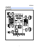
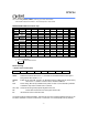
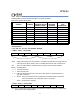
BLOCK DIAGRAM
P3.0
~
P3.7
P1.0
~
P1.7
ALU
Port 0
Latch
Port 1
Latch
Timer
1
Timer
0
Timer
2
Port
1
UART
XTAL1 PSENALE GNDVCCRSTXTAL2
Oscillator
Interrupt
PSW
16KB
ROM
Instruction
Decoder
&
Sequencer
Reset Block
Bus & Clock
Controller
SFR RAM
Address
Power control
256 bytes
RAM & SFR
Stack
Pointer
B
Addr. Reg.
Incrementor
PC
DPTR
Temp Reg.
T2T1
ACC
Port 3
Latch
Port 4
Latch
Port
3
Port 2
Latch
P4.0
~
P4.3
Port
4
Port
0
Port
2
P2.0
~
P2.7
P0.0
~
P0.7
INT2
INT3
Figure 2. Architecture of the W78C54