
Manual

W78C54
Publication Release Date: December 1997
- 5 - Revision A2
FUNCTIONAL DESCRIPTION
The W78C54 is pin-to-pin compatible with the W78C52, except that the internal 8K mask ROM has
been replaced with 16K of internal mask ROM. The processor supports 111 different opcodes and
references both 64K program address space and 64K data storage space.
Clock
The W78C54 is designed to be used with either a crystal oscillator or an external clock. Internally, the
clock is divided by two before it is used. This makes the W78C54 relatively insensitive to duty cycle
variations in the clock.
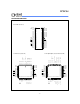
Crystal Oscillator
The W78C54 incorporates a built-in crystal oscillator. To make the oscillator work, a crystal is
connected across pins XTAL1 and XTAL2. In addition, a load capacitance of 30 pf (typically) must be
connected from each pin to ground. Resistor must also be connected from XTAL1 to XTAL2 to
provide a DC bias when the crystal frequency is above 24 MHz.
External Clock
An external clock should be connected to pin XTAL1. Pin XTAL2 should be left unconnected. The
XTAL1 input is a CMOS-type input, as required by the crystal oscillator. As a result, the external clock
signal should have an input one level greater than 3.5 volts.
Power Management
Idle Mode
The idle mode is entered by setting the IDLE bit in the PCON register. In the idle mode, the internal
clock to the processor is stopped. The peripherals and the interrupt logic continue to be clocked. The
processor will exit idle mode when either an interrupt or a reset occurs.
Power-down Mode
When the PD bit of the PCON register is set, the processor enters the power-down mode. In this
mode all of the clocks are stopped, including the oscillator. The only way to exit power-down mode is
by a reset.
Reset
The external RESET signal is sampled at S5P2. To take effect, it must be held high for at least two
machine cycles while the oscillator is running.
An internal trigger circuit in the reset line is used to deglitch the reset line when the
W78C54 is used
with an external RC network. The reset logic also has a special glitch removal circuit that ignores
glitches on the reset line.
During reset, the ports are initialized to FFH, the stack pointer to 07H, PCON (with the exception of
bit 4) to 00H, and all of the other SFR registers except SBUF to 00H. SBUF is not reset.
New Defined Peripheral
In order to be more suitable for I/O, an extra 4-bit bit-addressable port P4 and two external interrupt
INT2, INT3 has been added to either the PLCC or QFP 44 pin package. And description follows: