
Instruction Manual


W78C58
Publication Release Date: December 1997
- 13 - Revision A5
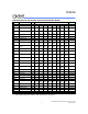
DC Characteristics, continued
PARAMETER SYM. SPECIFICATION UNIT TEST CONDITIONS
MIN. MAX.
Input Low Voltage
P0, P1, P2, P3, P4,
EA
VIL1 0 0.8 V VDD = 4.5V
Input Low Voltage
RST
VIL2 0 0.8 V VDD = 4.5V
Input Low Voltage
XTAL1[*4]
VIL3 0 0.8 V VDD = 4.5V
Input High Voltage
P0, P1, P2, P3, P4,
EA
VIH1 2.4 VDD +0.2 V VDD = 5.5V
Input High Voltage
RST
VIH2 3.5 VDD +0.2 V VDD = 5.5V
Input High Voltage
XTAL1 [*4]
VIH3 3.5 VDD +0.2 V VDD = 5.5V
Output Low Voltage
P1, P2, P3, P4
VOL1 - 0.45 V VDD = 4.5V
I
OL = +2 mA
Output Low Voltage
P0, ALE,
PSEN [*3]
V
OL2 - 0.45 V VDD = 4.5V
I
OL = +4 mA
Sink Current
P1, P2, P3, P4
ISK1 48mAVDD = 4.5V
Vs = 0.45V
Sink Current
P0, ALE,
PSEN
I
SK2 10 14 mA VDD = 4.5V
Vs = 0.45V
Output High Voltage
P1, P2, P3, P4
VOH1 2.4 - V VDD = 4.5V
I
OH = -100 µA
Output High Voltage
P0, ALE,
PSEN [*3]
V
OH2 2.4 - V VDD = 4.5V
I
OH = -400 µA
Source Current
P1, P2, P3, P4
ISR1 -120 -180
µA
VDD = 4.5V
Vs = 2.4V
Source Current
P0, ALE,
PSEN
I
SR2 -8 -14 mA VDD = 4.5V
Vs = 2.4V
Notes:
*1. RST pin is a Schmitt trigger input. RST has internal pull-low resistors of about 30 KΩ.
*3. P0, ALE and /PSEN are tested in the external access mode.
*4. XTAL1 is a CMOS input.
*5. Pins of P1, P2, P3, P4 can source a transition current when they are being externally driven from 1 to 0. The transition
current reaches its maximum value when V
IN approximates to 2V.