
User guide

W78C801
- 4 -
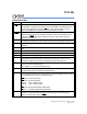
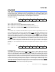
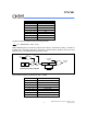
BLOCK DIAGRAM
P3.0
P3.7
P1.0
P1.7
ALU
Port 0
Latch
Port 1
Latch
Timer
1
Timer
0
Port
1
XTAL1
PSEN
ALE
VssVCCRSTXTAL2
Oscillator
Interrupt
PSW
Instruction
Decoder
&
Sequencer
Reset Block
Bus & Clock
Controller
SFR RAM
Address
Power control
256 bytes
RAM & SFR
Stack
Pointer
B
Addr. Reg.
Incrementor
PC
DPTR
Temp Reg.
T2T1
ACC
Port 3
Latch
Port 4
Latch
Port
3
Port 2
Latch
P4.0
P4.6
Port
4
Port
0
Port
2
P2.0
P2.7
P0.0
P0.7
INT2~9
Watchdog
Timer
FUNCTIONAL DESCRIPTION
The W78C801 architecture consists of a core controller surrounded by various registers, five general
purpose I/O ports, 256 bytes of RAM, two timer/counters. The processor supports 111 different
opcodes and references both a 64K program address space and a 64K data storage space.
Timers 0, 1
Timers 0, 1 each consist of two 8-bit data registers. These are called TL0 and TH0 for Timer 0, TL1
and TH1 for Timer 1. The TCON and TMOD registers provide control functions for timers 0 and 1.
The operations of Timer 0 and Timer 1 are the same as in the W78C51.
I/O Port Options
The Port 0 and Port 3 of W78C801 may be configured with different types by setting the bits of the
Port Options Register POR that is located at 86H. The pins of Port 0 can be configured with either the
open drain or standard port with internal pull-up. By the default, Port 0 is an open drain bi-directional
I/O port. When the PUP bit in the POR register is set, the pins of Port 0 will perform a quasi-bi-
directional I/O port with internal pull-up that is structurally the same as Port 2. The high nibble of Port