Preliminary W79E8213/W79E8213R Data Sheet 8-BIT MICROCONTROLLER Table of Contents1. 2. 3. 4. 5. 6. GENERAL DESCRIPTION ......................................................................................................... 4 FEATURES ................................................................................................................................. 5 PARTS INFORMATION LIST ..................................................................................................... 6 3.
Preliminary W79E8213/W79E8213R Data Sheet 11.1.3 12. 13. 11.2 Reset State ................................................................................................................... 55 INTERRUPTS ........................................................................................................................... 56 12.1 Interrupt Sources .......................................................................................................... 56 12.2 Priority Level Structure ...............
Preliminary W79E8213/W79E8213R Data Sheet 27. 28. 26.1 Absolute Maximum Ratings .......................................................................................... 90 26.2 DC ELECTRICAL CHARACTERISTICS ...................................................................... 90 26.3 The ADC Converter DC ELECTRICAL CHARACTERISTICS ..................................... 92 26.4 Internal RC Oscillator Accuracy DC ELECTRICAL CHARACTERISTICS ................... 92 26.5 AC ELECTRICAL CHARACTERISTICS .......
Preliminary W79E8213/W79E8213R Data Sheet 1. GENERAL DESCRIPTION The W79E8213 series are an 8-bit 4T-8051 microcontroller which has Flash EPROM which is programmable by ICP (In Circuit Program) or by hardware writer. The instruction set of the W79E8213 series are fully compatible with the standard 8052. The W79E8213 series contain a 4K bytes of main Flash EPROM; a 128 bytes of RAM; two 16-bit timer/counters; 4-channel 10-bit PWM; 3 edge detector inputs; 8-channel multiplexed 10-bit A/D convert.
Preliminary W79E8213/W79E8213R Data Sheet 2. FEATURES z z z Fully static design 8-bit 4T-8051 CMOS microcontroller: VDD = 4.5V to 5.5V @20MHz VDD = 2.7V to 5.5V @12MHz VDD = 2.4V to 5.5V @4MHz Instruction-set compatible with MSC-51. Flexible CPU clock source configurable by config bit and software: High speed external oscillator: upto 20MHz Crystal and resonator (enabled by config bit).
Preliminary W79E8213/W79E8213R Data Sheet 3. PARTS INFORMATION LIST 3.1 Lead Free (RoHS) Parts information list EPROM FLASH SIZE RAM NVM FLASH EPROM INTERNAL RC OSCILLATOR ACCURACY PACKAGE W79E8213AKG 4KB 128B 128B ±25% DIP-20 Pin W79E8213ASG 4KB 128B 128B ±25% SOP-20 Pin W79E8213RAKG 4KB 128B 128B ±2% DIP-20 Pin W79E8213RASG 4KB 128B 128B ±2% SOP-20 Pin PART NO. Table 3-1: Lead Free (RoHS) Parts information list 4.
Preliminary W79E8213/W79E8213R Data Sheet 5. PIN DESCRIPTIONS SYMBOL ALTERNATE ALTERNATE ALTERNATE ALTERNATE FUNCTION 4 FUNCTION 1 FUNCTION 2 FUNCTION 3 (ICP MODE) VDD VSS TYPE P POWER SUPPLY: Supply voltage for operation. P GROUND: Ground potential. P0.0 AD6 PWM3 I/O P0.1 AD5 PWM0 I/O P0.2 AD4 BRAKE I/O P0.3 AD0 P0.4 AD1 Data I/O P0.5 AD2 Clock I/O P0.6 AD3 P0.7 AD7 P1.0 BUZ P1.1 DESCRIPTIONS I/O Port0: Support 4 output modes and TTL/Schmitt trigger.
Preliminary W79E8213/W79E8213R Data Sheet 6. FUNCTIONAL DESCRIPTION The W79E8213 series architecture consist of a 4T 8051 core controller surrounded by various registers, 4K bytes Flash EPROM, 128 bytes of RAM, up to 18 general purpose I/O ports, two timer/counters, 3 edge detector inputs, 4-channel PWM with 10-bits counter, 8-channel multiplexed with 10-bit ADC analog input, Flash EPROM program by Writer and ICP. W79E8213 series supported 128 bytes NVM Data Flash EPROM. 6.
Preliminary W79E8213/W79E8213R Data Sheet 6.6.1 ALU The ALU is the heart of the W79E8213 series. It is responsible for the arithmetic and logical functions. It is also used in decision making, in case of jump instructions, and is also used in calculating jump addresses. The user cannot directly use the ALU, but the Instruction Decoder reads the op-code, decodes it, and sequences the data through the ALU and its associated registers to generate the required result.
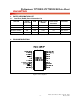
Preliminary W79E8213/W79E8213R Data Sheet 7. MEMORY ORGANIZATION The W79E8213 series separate the memory into two separate sections, the Program Memory and the Data Memory. The Program Memory is used to store the instruction op-codes, while the Data Memory is used to store data or for memory mapped devices.
Preliminary W79E8213/W79E8213R Data Sheet 7.3 Data Memory (accessed by MOVX) Not available in this product series. 7.4 Scratch-pad RAM and Register Map As mentioned before the W79E8213 series have separate Program and Data Memory areas. The onchip 128 bytes scratch pad RAM is in addition to the external memory. There are also several Special Function Registers (SFRs) which can be accessed by software.
Preliminary W79E8213/W79E8213R Data Sheet FFH Indirect RAM 80H 7FH Direct RAM 30H 2FH 7F 7E 7D 7C 7B 7A 79 78 2EH 77 76 75 74 73 72 71 70 2DH 6F 6E 6D 6C 6B 6A 69 68 2CH 67 66 65 64 63 62 61 60 2BH 5F 5E 5D 5C 5B 5A 59 58 2AH 57 56 55 54 53 52 51 50 29H 4F 4E 4D 4C 4B 4A 49 48 28H 47 46 45 44 43 42 41 40 27H 3F 3E 3D 3C 3B 3A 39 38 33 32 31 30 26H 37 36 35 34 25H 2F 2E 2D 2C 2B 2A 29 28 24H 27 26 25 24 2
Preliminary W79E8213/W79E8213R Data Sheet 7.4.2 Bit addressable Locations The Scratch-pad RAM area from location 20h to 2Fh is byte as well as bit addressable. This means that a bit in this area can be individually addressed. In addition some of the SFRs are also bit addressable. The instruction decoder is able to distinguish a bit access from a byte access by the type of the instruction itself. In the SFR area, any existing SFR whose address ends in a 0 or 8 is bit addressable. 7.4.
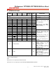
Preliminary W79E8213/W79E8213R Data Sheet 8. SPECIAL FUNCTION REGISTERS The W79E8213 series uses Special Function Registers (SFRs) to control and monitor peripherals and their Modes. The SFRs reside in the register locations 80-FFh and are accessed by direct addressing only. Some of the SFRs are bit addressable. This is very useful in cases where users wish to modify a particular bit without changing the others. The SFRs that are bit addressable are those whose addresses end in 0 or 8.
Preliminary W79E8213/W79E8213R Data Sheet BIT_ADDRESS, SYMBOL ADD MSB RESS LSB RESET SYMBOL DEFINITION BUZCON Square wave control register F9H - - BUZDIV. BUZDIV. BUZDIV. BUZDIV. BUZDIV. BUZDIV.
Preliminary W79E8213/W79E8213R Data Sheet Continued BIT_ADDRESS, SYMBOL DEFINITION ADD MSB RESS LSB IP0H Interrupt high priority B7H - PADCH PBOH - PT1H PX1H PT0H PX0H x00x0000B P2M2 Port 2 output mode 2 B6H - - - - - - P2M2.1 P2M2.0 xxxxxx 00B P2M1 Port 2 output mode 1 B5H P2S P1S P0S ENCLK T1OE T0OE P2M2.1 P2M2.0 00000000B P1M2 Port 1 output mode 2 B4H P1M2.7 P1M2.6 - P1M2.4 P1M2.3 P1M2.2 P1M2.1 P1M2.0 00x00000B P1M1 Port 1 output mode 1 B3H P1M1.
Preliminary W79E8213/W79E8213R Data Sheet PORT 0 Bit: 7 6 5 4 3 2 1 0 P0.7 P0.6 P0.5 P0.4 P0.3 P0.2 P0.1 P0.0 Mnemonic: P0 Address: 80h P0.7-0: General purpose Input/Output port. Most instructions will read the port pins in case of a port read access, however in case of read-modify-write instructions, the port latch is read. These alternate functions are described below: BIT NAME FUNCTION 7 P0.7 AD7 pin or Timer 1 pin by alternative. 6 P0.6 AD3 pin by alternative. 5 P0.
Preliminary W79E8213/W79E8213R Data Sheet DATA POINTER HIGH Bit: 7 6 5 4 3 2 1 0 DPH.7 DPH.6 DPH.5 DPH.4 DPH.3 DPH.2 DPH.1 DPH.0 Mnemonic: DPH BIT NAME 7-0 DPH.[7:0] Address: 83h FUNCTION This is the high byte of the standard 8052 16-bit data pointer. This is the high byte of the DPTR 16-bit data pointer. POWER CONTROL Bit: 7 6 5 4 3 2 1 0 - - BOF POR GF1 GF0 PD IDL Mnemonic: PCON BIT Address: 87h NAME FUNCTION 7 - Reserved. 6 - Reserved.
Preliminary W79E8213/W79E8213R Data Sheet BIT NAME FUNCTION 7 TF1 Timer 1 Overflow Flag. This bit is set when Timer 1 overflows. It is cleared automatically when the program does a timer 1 interrupt service routine. Software can also set or clear this bit. 6 TR1 Timer 1 Run Control. This bit is set or cleared by software to turn timer/counter on or off. 5 TF0 Timer 0 Overflow Flag. This bit is set when Timer 0 overflows.
Preliminary W79E8213/W79E8213R Data Sheet M1 M0 MODE 0 0 Mode 0: 13-bits timer/counter; THx 8 bits and TLx 5 bits which serve as pre-scalar. 0 1 Mode 1: 16-bit timer/counter, no pre-scale. 1 0 Mode 2: 8-bit timer/counter with auto-reload from THx. 1 1 Mode 3: (Timer 0) TL0 is an 8-bit timer/counter controlled by the standard Timer0 control bits. TH0 is an 8-bit timer only controlled by Timer1 control bits. (Timer 1) Timer/Counter 1 is stopped. TIMER 0 LSB Bit: 7 6 5 4 3 2 1 0 TL0.
Preliminary W79E8213/W79E8213R Data Sheet CLOCK CONTROL Bit: 7 6 5 4 3 2 1 0 - - - T1M T0M - - - Mnemonic: CKCON Address: 8Eh BIT NAME FUNCTION 7-5 - 4 T1M Timer 1 clock select: 0: Timer 1 uses a divide by 12 clocks. 1: Timer 1 uses a divide by 4 clocks. 3 T0M Timer 0 clock select: 0: Timer 0 uses a divide by 12 clocks. 1: Timer 0 uses a divide by 4 clocks. 2-0 - Reserved. Reserved. PORT 1 Bit: 7 6 5 4 3 2 1 0 P1.7 P1.6 P1.5 P1.4 P1.3 P1.2 P1.1 P1.
Preliminary W79E8213/W79E8213R Data Sheet BIT NAME FUNCTION 7-2 - 1 P2.1 XTAL1 clock input pin. 0 P2.0 XTAL2 or CLKOUT pin by alternative. Reserved. Note: During power-on-reset, the port pins are tri-stated. After power-on-reset, the value of the port is set by CONFIG0.PRHI bit. The default setting for CONFIG0.PRHI =1 which the alternative function output is turned on upon reset. If CONFIG0.PRHI is set to 0, the user has to write a 1 to port SFR to turn on the alternative function output.
Preliminary W79E8213/W79E8213R Data Sheet EDGE DETECT CONTROL REGISTER Bit: 7 6 5 4 3 2 1 0 EDFILT.1 EDFILT.0 ED2TRG ED2EN ED1TRG ED1EN ED0TRG ED0EN Mnemonic: EDIC BIT Address: A3h NAME FUNCTION Edge detect filter type bits: 00 – Filter clock = Fosc. 01 – Filter clock = Fosc/2. 10 – Filter clock = Fosc/4. 11 – Filter clock = Fosc/8. 7-6 ED2TRG Edge detect 2 (ED2) trigger type bit: 0 – Falling edge on ED2 pin will cause EDF to be set (if ED2EN is enabled).
Preliminary W79E8213/W79E8213R Data Sheet BIT NAME FUNCTION 7 EA Global enable. Enable/Disable all interrupts. 6 EADC Enable ADC interrupt. 5 EBO Enable Brown Out interrupt. 4 - Reserved. 3 ET1 Enable Timer 1 interrupt. 2 EX1 Enable external interrupt 1. 1 ET0 Enable Timer 0 interrupt. 0 EX0 Enable external interrupt 0. PORT 0 OUTPUT MODE 1 Bit: 7 6 5 4 3 2 1 0 P0M1.7 P0M1.6 P0M1.5 P0M1.4 P0M1.3 P0M1.2 P0M1.1 P0M1.0 Mnemonic: P0M1 BIT NAME 7-0 P0M1.
Preliminary W79E8213/W79E8213R Data Sheet PORT 2 OUTPUT MODE 1 Bit: 7 6 5 4 3 2 1 0 P2S P1S P0S ENCLK T1OE T0OE P2M1.1 P2M1.0 Mnemonic: P2M1 BIT Address: B5h NAME FUNCTION 7 P2S 0: Disable Schmitt trigger inputs on port 2 and enable TTL inputs on port 2. 1: Enables Schmitt trigger inputs on Port 2. 6 P1S 0: Disable Schmitt trigger inputs on port 1 and enable TTL inputs on port 1. 1: Enables Schmitt trigger inputs on Port 1.
Preliminary W79E8213/W79E8213R Data Sheet INTERRUPT HIGH PRIORITY Bit: 7 6 5 4 3 2 1 0 - PADCH PBOH - PT1H PX1H PT0H PX0H Mnemonic: IP0H BIT Address: B7h NAME FUNCTION 7 - This bit is un-implemented and will read high. 6 PADCH 1: To set interrupt high priority of ADC is highest priority level. 5 PBOH 1: To set interrupt high priority of Brown Out Detector is highest priority level. 4 - Reserved. 3 PT1H 1: To set interrupt high priority of Timer 1 is highest priority level.
Preliminary W79E8213/W79E8213R Data Sheet BIT 7 6~0 NAME FUNCTION - Please Keep it at 0. NVMADDR.[7:0] The NVM address: The register indicates NVM data memory address on On-Chip code memory space. TIMED ACCESS Bit: 7 6 5 4 3 2 1 0 TA.7 TA.6 TA.5 TA.4 TA.3 TA.2 TA.1 TA.0 Mnemonic: TA BIT 7-0 Address: C7h NAME TA.[7:0] FUNCTION The Timed Access register: The Timed Access register controls the access to protected bits.
Preliminary W79E8213/W79E8213R Data Sheet BIT NAME FUNCTION 7~0 NVMDATA.[7:0] The NVM data write register. The read NVM data is by MOVC instruction. PROGRAM STATUS WORD Bit: 7 6 5 4 3 2 1 0 CY AC F0 RS1 RS0 OV F1 P Mnemonic: PSW BIT Address: D0h NAME FUNCTION CY Carry flag: Set for an arithmetic operation which results in a carry being generated from the ALU. It is also used as the accumulator for the bit operations.
Preliminary W79E8213/W79E8213R Data Sheet BIT NAME FUNCTION 7-2 - Reserved. 1-0 PWMP.[9:8] The PWM Counter Register bits 9~8. PWM 0 HIGH BITS REGISTER Bit: 7 6 5 4 3 2 1 0 - - - - - - PWM0.9 PWM0.8 Mnemonic: PWM0H BIT Address: D2h NAME FUNCTION 7~2 - Reserved. 1~0 PWM0.[9:8] The PWM 0 High Bits Register bit 9~8. PWM 1 HIGH BITS REGISTER Bit: 7 6 5 4 3 2 1 0 - - - - - - PWM1.9 PWM1.8 Mnemonic: PWM1H BIT Address: D3h NAME FUNCTION 7~2 - Reserved.
Preliminary W79E8213/W79E8213R Data Sheet PWM CONTROL REGISTER 3 Bit: 7 6 - - 5 4 - - 3 2 1 0 FP1 FP0 - BKF Mnemonic: PWMCON3 BIT NAME 7-4 - 3-2 FP[1:0] 1 - 0 BKF Address: D7h FUNCTION Reserved. Select PWM frequency pre-scale select bits. The clock source of pre-scaler, Fpwm is in phase with Fosc if PWMRUN=1. FP[1:0] Fpwm 00 FOSC 01 FOSC/2 10 FOSC/4 11 FOSC/16 Reserved. The external brake pin flag: 0: The PWM is not brake. 1: The PWM is brake by external brake pin.
Preliminary W79E8213/W79E8213R Data Sheet Continued BIT NAME 2 WTRF 1 EWRST 0 WDCLR FUNCTION Watchdog Timer Reset Flag 1: Hardware will set this bit when the watchdog timer causes a reset. Software can read it but must clear it manually. A power-fail reset will also clear the bit. This bit helps software in determining the cause of a reset. If EWRST = 0, the watchdog timer will have no affect on this bit. 0: Disable Watchdog Timer Reset. 1: Enable Watchdog Timer Reset.
Preliminary W79E8213/W79E8213R Data Sheet Continued BIT 0 NAME FUNCTION Reset Watchdog Timer This bit helps in putting the watchdog timer into a know state. It also helps in resetting the watchdog timer before a time-out occurs. Failing to set the EWRST before time-out will cause an interrupt, if EWDI (EIE.4) is set, and 512 clocks after that a watchdog timer reset will be generated if EWRST is set. This bit is self-clearing by hardware. WDCLR The WDCON SFR is set to 0x000000B on a reset.
Preliminary W79E8213/W79E8213R Data Sheet BIT NAME 7~0 PWM1.[7:0] FUNCTION PWM 1 Low Bits Register. PWM CONTROL REGISTER 1 Bit: 7 6 5 4 3 2 1 0 PWMRUN Load PWMF CLRPWM - - PWM1I PWM0I Mnemonic: PWMCON1 Address: DCh BIT NAME 7 PWMRUN 0: The PWM is not running. 1: The PWM counter is running. Load 0: The registers value of PWMP and PWMn are never loaded to counter and Comparator registers.
Preliminary W79E8213/W79E8213R Data Sheet PWM3 LOW BITS REGISTER Bit: 7 6 5 4 3 2 1 0 PWM3.7 PWM3.6 PWM3.5 PWM3.4 PWM3.3 PWM3.2 PWM3.1 PWM3.0 Mnemonic: PWM3L BIT NAME 7~0 PWM3.[7:0] Address: DEh FUNCTION PWM 3 Low Bits Register. PWM CONTROL REGISTER 2 Bit: 7 6 5 4 3 2 1 0 BKCH BKPS BPEN BKEN PWM3B PWM2B PWM1B PWM0B Mnemonic: PWMCON2 BIT Address: DFh NAME FUNCTION 7 BKCH See the below table, when BKEN is set. 6 BKPS 0: Brake is asserted if P0.2 is low.
Preliminary W79E8213/W79E8213R Data Sheet Brake Condition Table: BPEN BKCH BRAKE CONDITION 0 Brake On (software brake and keeping brake). Software brake condition. When active (BPEN=BKCH=0, and BKEN=1), PWM output follows PWMnB setting. This brake has no effect on PWMRUN bit, therefore, internal PWM generator continues to run. When the brake is released, the state of PWM output depends on the current state of PWM generator output during the release.
Preliminary W79E8213/W79E8213R Data Sheet BIT NAME 7-6 ADC.1-0 2 LSB of 10-bit A/D conversion result. ADCEX Enable STADC-triggered conversion 0: Conversion can only be started by software (i.e., by setting ADCS). 1: Conversion can be started by software or by a rising edge on STADC (pin P1.4). ADCI ADC Interrupt flag: This flag is set when the result of an A/D conversion is ready. This generates an ADC interrupt, if it is enabled. The flag may be cleared by the ISR.
Preliminary W79E8213/W79E8213R Data Sheet AADR1, AADR0: ADC Analog Input Channel select bits: These bits can only be changed when ADCI and ADCS are both zero. AADR2 AADR1 AADR0 SELECTED ANALOG INPUT CHANNEL 0 0 0 AD0 (P0.3) 0 0 1 AD1 (P0.4) 0 1 0 AD2 (P0.5) 0 1 1 AD3 (P0.6) 1 0 0 AD4 (P0.2) 1 0 1 AD5 (P0.1) 1 1 0 AD6 (P0.0) 1 1 1 AD7 (P0.7) ADC CONVERTER RESULT HIGH REGISTER Bit: 7 6 5 4 3 2 1 0 ADC.9 ADC.8 ADC.7 ADC.6 ADC.5 ADC.4 ADC.3 ADC.
Preliminary W79E8213/W79E8213R Data Sheet Bit: 7 6 5 4 3 2 1 0 EED EPWMUF EPWM EWDI - - - - Mnemonic: EIE BIT Address: E8h NAME FUNCTION 7 EED 0: Disable Edge Detect Interrupt. 1: Enable Edge Detect Interrupt. 6 EPWMUF 0: Disable PWM underflow interrupt. 1: Enable PWM underflow interrupt. 5 EPWM 0: Disable PWM Interrupt when external brake pin was brake. 1: Enable PWM Interrupt when external brake pin was brake. 4 EWDI 0: Disable Watchdog Timer Interrupt.
Preliminary W79E8213/W79E8213R Data Sheet Continued BIT NAME 4 PADIDS.4 P0.4 digital input disable bit. 0: Default (With digital/analog input). 1: Disable Digital Input of ADC Input Channel 1. PADIDS.3 P0.3 digital input disable bit. 0: Default (With digital/analog input). 1: Disable Digital Input of ADC Input Channel 0. 2 PADIDS.2 P0.2 digital input disable bit. 0: Default (With digital/analog input). 1: Disable Digital Input of ADC Input Channel 4. 1 PADIDS.1 P0.1 digital input disable bit.
Preliminary W79E8213/W79E8213R Data Sheet BIT NAME FUNCTION 7 PED 1: To set interrupt priority of Edge Detect is higher priority level. 6 PPWM 1: To set interrupt priority of PWM underflow is higher priority level. 5 PBK 1: To set interrupt priority of PWM’s external brake is higher priority level. 4 PWDI 1: To set interrupt priority of Watchdog is higher priority level. - Reserved. 3-0 BUZZER CONTROL REGISTER Bit: 7 6 5 4 3 2 1 0 - - BUZDIV.5 BUZDIV.4 BUZDIV.3 BUZDIV.
Preliminary W79E8213/W79E8213R Data Sheet 9. INSTRUCTION SET The W79E8213 series execute all the instructions of the standard 8052 family. The operations of these instructions, as well as their effects on flag and status bits, are exactly the same. However, the timing of these instructions is different in two ways. Firstly, the machine cycle is four clock periods, while the standard-8051/52 machine cycle is twelve clock periods. Secondly, it can fetch only once per machine cycle (i.e.
Preliminary W79E8213/W79E8213R Data Sheet INSTRUCTION SET, continued Op-code HEX Code Bytes W79E8213 series Machine Cycle W79E8213 series Clock cycles 8032 Clock cycles W79E8213 series vs. 8032 Speed Ratio ADDC A, #data 34 2 2 8 12 1.
Preliminary W79E8213/W79E8213R Data Sheet INSTRUCTION SET, continued Op-code HEX Code Bytes W79E8213 series Machine Cycle W79E8213 series Clock cycles 8032 Clock cycles W79E8213 series vs. 8032 Speed Ratio DEC R7 1F 1 1 4 12 3 DEC @R0 16 1 1 4 12 3 DEC @R1 17 1 1 4 12 3 DEC direct 15 2 2 8 12 1.5 DEC DPTR A5 1 2 8 24 3 MUL AB A4 1 5 20 48 2.4 DIV AB 84 1 5 20 48 2.
Preliminary W79E8213/W79E8213R Data Sheet INSTRUCTION SET, continued Op-code HEX Code Bytes W79E8213 series Machine Cycle W79E8213 series Clock cycles 8032 Clock cycles W79E8213 series vs. 8032 Speed Ratio ORL direct, A 42 2 2 8 12 1.
Preliminary W79E8213/W79E8213R Data Sheet INSTRUCTION SET, continued Op-code HEX Code Bytes W79E8213 series Machine Cycle W79E8213 series Clock cycles 8032 Clock cycles W79E8213 series vs. 8032 Speed Ratio MOV A, #data 74 2 2 8 12 1.
Preliminary W79E8213/W79E8213R Data Sheet INSTRUCTION SET, continued Op-code HEX Code Bytes W79E8213 series Machine Cycle W79E8213 series Clock cycles 8032 Clock cycles W79E8213 series vs. 8032 Speed Ratio MOV direct, R2 8A 2 2 8 12 1.5 MOV direct, R3 8B 2 2 8 12 1.5 MOV direct, R4 8C 2 2 8 12 1.5 MOV direct, R5 8D 2 2 8 12 1.5 MOV direct, R6 8E 2 2 8 12 1.5 MOV direct, R7 8F 2 2 8 12 1.5 MOV direct, @R0 86 2 2 8 12 1.
Preliminary W79E8213/W79E8213R Data Sheet INSTRUCTION SET, continued Op-code HEX Code Bytes W79E8213 series Machine Cycle W79E8213 series Clock cycles 8032 Clock cycles W79E8213 series vs. 8032 Speed Ratio CLR C C3 1 1 4 12 3 CLR bit C2 2 2 8 12 1.5 SETB C D3 1 1 4 12 3 SETB bit D2 2 2 8 12 1.5 CPL C B3 1 1 4 12 3 CPL bit B2 2 2 8 12 1.
Preliminary W79E8213/W79E8213R Data Sheet INSTRUCTION SET, continued Op-code HEX Code Bytes W79E8213 series Machine Cycle W79E8213 series Clock cycles 8032 Clock cycles W79E8213 series vs. 8032 Speed Ratio CJNE R0, #data, rel B8 3 4 16 24 1.5 CJNE R1, #data, rel B9 3 4 16 24 1.5 CJNE R2, #data, rel BA 3 4 16 24 1.5 CJNE R3, #data, rel BB 3 4 16 24 1.5 CJNE R4, #data, rel BC 3 4 16 24 1.5 CJNE R5, #data, rel BD 3 4 16 24 1.
Preliminary W79E8213/W79E8213R Data Sheet 9.1 Instruction Timing This section is important because some applications use software instructions to generate timing delays. It also provides more information about timing differences between the W79E8213 series and the standard 8051/52. In W79E8213 series, each machine cycle is four clock periods long. Each clock period is called a state, and each machine cycle consists of four states: C1, C2 C3 and C4, in order.
Preliminary W79E8213/W79E8213R Data Sheet Operand Fetch Instruction Fetch C1 C2 C3 C4 C1 C2 C3 C4 CPU CLK ALE PSEN PC AD<7:0> Address<15:0> OP-CODE PC+1 Address A15-8 OPERAND Address A15-8 Figure 9-2: Two Cycles Instruction Timing Instruction Fetch C1 C2 C3 Operand Fetch C4 C1 C2 C3 Operand Fetch C4 C1 C2 C3 C4 CPU CLK ALE PSEN AD<7:0> Address<15:0> A7-0 OP-CODE Address A15-8 A7-0 OPERAND Address A15-8 A7-0 OPERAND Address A15-8 Figure 9-3: Three Cycles Instruction Tim
Preliminary W79E8213/W79E8213R Data Sheet Instruction Fetch C1 C2 C3 Operand Fetch C4 C1 C2 C3 Operand Fetch C4 C1 C2 C3 Operand Fetch C4 C1 C2 C3 C4 CPU CLK ALE PSEN AD<7:0> A7-0 Address<15:0> A7-0 OP-CODE A7-0 OPERAND Address A15-8 Address A15-8 A7-0 OPERAND Address A15-8 OPERAND Address A15-8 Figure 9-4: Four Cycles Instruction Timing Instruction Fetch C1 C2 C3 C4 Operand Fetch C1 C2 C3 C4 Operand Fetch C1 C2 C3 C4 Operand Fetch C1 C2 C3 C4 Operand Fetch C
Preliminary W79E8213/W79E8213R Data Sheet 10. POWER MANAGEMENT The W79E8213 series has several features that help the user to control the power consumption of the device. These modes are discussed in the next two sections. 10.1 Idle Mode The user can put the device into idle mode by writing 1 to the bit PCON.0. The instruction that sets the idle bit is the last instruction that will be executed before the device goes into Idle Mode.
Preliminary W79E8213/W79E8213R Data Sheet 11. RESET CONDITIONS The user has several hardware related options for placing the W79E8213 series into reset condition. In general, most register bits go to their reset value irrespective of the reset condition, but there are a few flags whose state depends on the source of reset. The user can use these flags to determine the cause of reset using software. 11.1 Sources of reset Figure 11-1: Reset and Vdd monitor timing diagram, disable /RST pin.
Preliminary W79E8213/W79E8213R Data Sheet Figure 11-2: Reset and Vdd monitor timing diagram, enable /RST pin. 11.1.1 External Reset The device samples the /RST pin every machine cycle during state C4. The /RST pin must be held low for at least two machine cycles before the reset circuitry applies an internal reset signal. Thus, this reset is a synchronous operation and requires the clock to be running.
Preliminary W79E8213/W79E8213R Data Sheet 11.1.3 Watchdog Timer Reset The Watchdog Timer is a free-running timer with programmable time-out intervals. The program must clear the Watchdog Timer before the time-out interval is reached to restart the count. If the time-out interval is reached, an interrupt flag is set. 512 clocks later, if the Watchdog Reset is enabled and the Watchdog Timer has not been cleared, the Watchdog Timer generates a reset.
Preliminary W79E8213/W79E8213R Data Sheet 12. INTERRUPTS The W79E8213 series have four priority level interrupts structure with 10 interrupt sources. Each of the interrupt sources has an individual priority bit, flag, interrupt vector and enable bit. In addition, the interrupts can be globally enabled or disabled. 12.1 Interrupt Sources The External Interrupts INT0 and INT1 can be either edge triggered or level triggered, programmable through bits IT0 and IT1.
Preliminary W79E8213/W79E8213R Data Sheet If any of these conditions are not met, then the LCALL will not be generated. The polling cycle is repeated every machine cycle, with the interrupts sampled in the same machine cycle. If an interrupt flag is active in one cycle but not responded to, and is not active when the above conditions are met, the denied interrupt will not be serviced. This means that active interrupts are not remembered; every polling cycle is new.
Preliminary W79E8213/W79E8213R Data Sheet 12.2 Priority Level Structure The W79E8213 series uses a four priority level interrupt structure (highest, high, low and lowest) and supports up to 10 interrupt sources. The interrupt sources can be individually set to either high or low levels. Naturally, a higher priority interrupt cannot be interrupted by a lower priority interrupt. However there exists a pre-defined hierarchy amongst the interrupts themselves.
Preliminary W79E8213/W79E8213R Data Sheet Continued Source Flag Vector address Interrupt Enable Bits Interrupt Priority Flag cleared by ADC Converter ADCI 005BH EAD (IE.6) IP0H.6, IP0.6 Hardware External Interrupt 1 IE1 0013H EX1 (IE.2) IP0H.2, IP0.2 Follow the Edge Detect Interrupt EDF 003BH EED (EIE.7) IP1H.7, IP1.7 Software Timer 1 Interrupt TF1 001BH ET1 (IE.3) IP0H.3, IP0.3 PWM Period Interrupt PWMF 006BH EPWMUF (EIE.6) IP1H.6, IP1.
Preliminary W79E8213/W79E8213R Data Sheet 12.4 Interrupt Inputs The W79E8213 series have total 10 interrupt sources with two individual interrupt inputs sources. They are IE0, IE1, BOF, EDF, WDT, TF0, TF1, BKF and ADC. Two interrupt inputs are identical to those present on the standard 80C51 microcontroller as show in below figures. If an external interrupt is enabled when the W79E8213 series are put into Power-down or Idle mode, the interrupt will cause the processor to wake up and resume operation.
Preliminary W79E8213/W79E8213R Data Sheet 13. PROGRAMMABLE TIMERS/COUNTERS The W79E8213 series have two 16-bit programmable timer/counters and one programmable Watchdog Timer. The Watchdog Timer is operationally quite different from the other two timers. Its’ timer/counters have additional timer 0 or timer 1 overflow toggle output enable feature as compare to conventional timer/counters.
Preliminary W79E8213/W79E8213R Data Sheet Figure 13-1: Timer/Counters 0 & 1 in Mode 0 13.1.3 Mode 1 Mode 1 is similar to Mode 0 except that the counting register forms a 16-bit counter, rather than a 13bit counter. This means that all the bits of THx and TLx are used. Roll-over occurs when the timer moves from a count of FFFFh to 0000h. The timer overflow flag TFx of the relevant timer is set and if enabled an interrupt will occur.
Preliminary W79E8213/W79E8213R Data Sheet 13.1.4 Mode 2 In Mode 2, the timer/counter is in the Auto Reload Mode. In this mode, TLx acts as 8-bit count register, while THx holds the reload value. When the TLx register overflows from FFh to 00h, the TFx bit in TCON is set and TLx is reloaded with the contents of THx, and the counting process continues from here. The reload operation leaves the contents of the THx register unchanged. Counting is enabled by the TRx bit and proper setting of GATE and INTx pins.
Preliminary W79E8213/W79E8213R Data Sheet Figure 13-4: Timer/Counter Mode 3 - 64 - Publication Release Date: July 11, 2008 Revision A2
Preliminary W79E8213/W79E8213R Data Sheet 14. NVM MEMORY The W79E8213 series have NVM data memory of 128 bytes for customer’s data store used. The NVM data memory has 8 pages area and each page of 16 bytes. The NVM memory can be read/write by customer program to access. Read NVM data is by MOVC A,@A+DPTR instruction, and write data is by SFR of NVMADDRL, NVMDATA and NVMCON.
Preliminary W79E8213/W79E8213R Data Sheet 15. WATCHDOG TIMER The Watchdog Timer is a free-running Timer which can be programmed by the user to serve as a system monitor, a time-base generator or an event timer. It is basically a set of dividers that divide the system clock. The divider output is selectable and determines the time-out interval. When the time-out occurs a flag is set, which can cause an interrupt if enabled, and a system reset can also be caused if it is enabled.
Preliminary W79E8213/W79E8213R Data Sheet any errant code is executed now, then the reset Watchdog Timer instructions will not be executed at the required instants and Watchdog reset will occur. The Watchdog Timer time-out selection will result in different time-out values depending on the clock speed. The reset, when enabled, will occur when 512 clocks after time-out has occurred.
Preliminary W79E8213/W79E8213R Data Sheet 16. TIME ACCESS PROCTECTION The W79E8213 series have a new feature, like the Watchdog Timer which is a crucial to proper operation of the system. If left unprotected, errant code may write to the Watchdog control bits resulting in incorrect operation and loss of control. In order to prevent this, the W79E8213 series have a protection scheme which controls the write access to critical bits. This protection scheme is done using a timed access.
Preliminary W79E8213/W79E8213R Data Sheet Example 5: Invalid Access MOV TA, #0AAh NOP MOV TA, #055h SETB EWT ; 3 M/C ; 1 M/C ; 3 M/C ; 2 M/C In the first three examples, the writing to the protected bits is done before the 3 machine cycles window closes. In Example 4, however, the writing to the protected bit occurs after the window has closed, and so there is effectively no change in the status of the protected bit.
Preliminary W79E8213/W79E8213R Data Sheet 17. EDGE DETECT INTERRUPT The W79E8213 series are provided edge detect interrupt function to detect keypad status which key is acted, and allow a single interrupt to be generated when any key is pressed on a keyboard or keypad connected to specific pins of the W79E8213 series, as shown below Figure. This interrupt may be used to wake up the CPU from Idle, after chip is in Idle Mode. Edge detect function is supported through Port 1.0-1.2.
Preliminary W79E8213/W79E8213R Data Sheet Figure 17-1: Edge Detect Interrupt Figure 17-2: Edge Detect Noise Filter - 71 - Publication Release Date: July 11, 2008 Revision A2
Preliminary W79E8213/W79E8213R Data Sheet 18. I/O PORT CONFIGURATION The W79E8213 series have three I/O ports, port 0, port 1 and port 2. All pins of I/O ports can be configured to one of four types by software except P1.5 is only input pin. When P1.5 is configured reset pin by RPD=0 in the CONFIG 1 register, the W79E8213 series can support 17 I/O pins by use Crystal. If used internal RC oscillator the P1.5 is configured input pin, the W79E8213 series can be supported up to 18 I/O pins.
Preliminary W79E8213/W79E8213R Data Sheet CPU clocks to pull high then turn off. The “weak” pull-up is turned on when the input port pin is logic “1” level or itself is logic “1”, and it provides the most source current for a quasi-bidirectional pin that output is “1” or port latch is logic “0”’. The “very weak” pull-up is turned on when the port latch is logic “1”. If port latch is logic “0”, it will be turned off.
Preliminary W79E8213/W79E8213R Data Sheet The push-pull output mode has two strong pull-up and pull-down structure that support large source and sink current output. It removes “weak” pull-up and “very weak” pull-up resister and remains “strong pull-up resister on quasi-bidirectional output mode. The “strong” pull-up is always turns on when port latch is logic “1” to support source current. The push-pull port configuration is shown in below Figure. Figure 18-3: Push-Pull Output 18.
Preliminary W79E8213/W79E8213R Data Sheet 19. OSCILLATOR The W79E8213 series provides three oscillator input option. These are configured at CONFIG register (CONFIG0) that include Internal RC Oscillator Option, External Clock Input Option and Crystal Oscillator Input Option. The Crystal Oscillator Input frequency may be supported from 4MHz to 20MHz, and without capacitor or resister. Figure 19-1: Oscillator 19.
Preliminary W79E8213/W79E8213R Data Sheet 20. BUZZER OUTPUT The W79E8213 series support square wave output capability. The square wave is output through P1.0 (BUZ) pin. The square wave can be enabled through bit BUZE (SFR AUXR1.1). Depending on Fcpu clock input to the buzzer output block, user is able to control the output frequency by configure the 6bit Divider through BUZDIV bits in BUZCON SFR. The following shows the block diagram of square wave output generator.
Preliminary W79E8213/W79E8213R Data Sheet Frequency, Fcpu (Hz) Division /256 4000000 6000000 8000000 10000000 11000000 12000000 15625 23437.5 31250 39062.5 42968.75 46875 20000000 78125 1 . 4 3906.25 5 6 3906.25 7 8 1953.125 3906.25 9 10 3906.25 11 12 3906.25 1953.125 3906.25 BUZDIV + 1 13 14 15 16 1953.125 17 18 19 20 1953.125 3906.25 21 22 1953.125 23 24 1953.125 25 . 40 1953.125 .
Preliminary W79E8213/W79E8213R Data Sheet For supporting active low buzzer, this buzzer output is implemented with an off-state of high. The following pseudo code shows the operating procedure when working with active high and low buzzer; (Assume PRHI=1): 1) During power on, P1.0/BUZ will be high; Clear SFR P1.0 ; user has to take care to output this pin low ; at the top of s/w code to avoid initial beep sound. No action needed.
Preliminary W79E8213/W79E8213R Data Sheet 21. POWER MONITORING FUNCTION Power-On Detect and Brownout are two additional power monitoring functions implemented in W79E8213 series to prevent incorrect operation during power up and power drop or loss. 21.1 Power On Detect The Power–On Detect function is a designed to detect power up after power voltage reaches to a level where Brownout Detect can work. After power on detect, the POR (PCON.4) will be set to “1” to indicate an initial power up condition.
Preliminary W79E8213/W79E8213R Data Sheet 22. PULSE-WIDTH-MODULATED (PWM) OUTPUTS The W79E8213 series have 4 Pulse Width Modulated (PWM) channels, and the PWM outputs are PWM0(P0.1), PWM1(P1.6), PWM2(P1.7), PWM3(P0.0). The initial PWM outputs level correspondingly depend on the PRHI level set prior to the chip reset. When PRHI set to high, PWM output will initialize to high after chip reset; if PRHI set to low, PWM output will be initialize to low after chip reset.
Preliminary W79E8213/W79E8213R Data Sheet 0 P0.2=0 1 P0.2=1 BKF BKCH Brake Control Block BPEN Enable External Brake Pin (BPEN,BKCH)=(1,X) PWMP Register BKPS BKEN load PWMRUN Counter Register Fosc D Posc Prescaler (1/1, 1/2, 1/4, 1/16) (FP1, FP0) SET CLR Fcpwm 10-bit Down Counter Underflow Q PWMF Q S/W Clear P0.1 X PWM0I + + Clear Counter CLRPWM Brake Pin (P0.2) 0 PWM0 (P0.1) > Y -- PWM0B 1 Compare Register P1.6 PWM0 register PWM1I X + 0 PWM1 (P1.
Preliminary W79E8213/W79E8213R Data Sheet PWMCON2.6 (BKPS) bit respectively. The details description of varies brake functions can be found in the brake condition table. Since the Brake Pin being asserted will automatically clear the Run bit of PWMCON1.7 and BKF (PWMCON3.0) flag will be set, the user program can poll this bit or enable PWM’s brake interrupt to determine when the Brake Pin causes a brake to occur.
Preliminary W79E8213/W79E8213R Data Sheet 23. ANALOG-TO-DIGITAL CONVERTER The ADC contains a DAC which converts the contents of a successive approximation register to a voltage (VDAC) which is compared to the analog input voltage (Vin). The output of the comparator is fed to the successive approximation control logic which controls the successive approximation register. A conversion is initiated by setting ADCS in the ADCCON register.
Preliminary W79E8213/W79E8213R Data Sheet Figure 23-1: Successive Approximation ADC 23.1 ADC Resolution and Analog Supply: The ADC circuit has its own supply pins (AVDD and AVSS) and one pins (Vref+) connected to each end of the DAC’s resistance-ladder that the AVDD and Vref+ are connected to VDD and AVSS is connected to VSS. The ladder has 1023 equally spaced taps, separated by a resistance of “R”. The first tap is located 0.5×R above AVSS, and the last tap is located 0.5×R below Vref+.
Preliminary W79E8213/W79E8213R Data Sheet Figure 23-2: ADC block diagram Note: As Port 0 is multi-function port, when configuring Port0 for ADC application, user should configure Input Only (High Impedance) and Disable Digital Input on port 0. This is done using P1Mx and PADIDS SFRs.
Preliminary W79E8213/W79E8213R Data Sheet 24. ICP (IN-CIRCUIT PROGRAM) FLASH PROGRAM The contexts of flash in W79E8213 series are empty by default. At the first use, you must program the flash EPROM by external Writer device or by ICP (In-Circuit Program) tool. Vcc ICP Power Jumper ICP Connector Vdd Vdd Vpp RST Data P0.4 Clock P0.5 Vss Jumper To Reset or Input Pin To I/O pin To I/O pin Vss W79E8213 Series System Board Note: 1. When using ICP to upgrade code, the P1.5, P0.4 and P0.
Preliminary W79E8213/W79E8213R Data Sheet 25. CONFIG BITS The W79E8213 series has two CONFIG bits (CONFIG0 located at FB00h, CONFIG1 located at FB01h) that must be defined at power up and can not be set the program after start of execution. Those features are configured through the use of two flash EPROM bytes, and the flash EPROM can be programmed and verified repeatedly. Until the code inside the Flash EPROM is confirmed OK, the code can be protected.
Preliminary W79E8213/W79E8213R Data Sheet Oscillator Configuration bits: Fosc1 Fosc0 OSC source 0 0 4MHz ~ 20MHz crystal 0 1 Internal RC Oscillator (FS1 bit in CONFIG1.
Preliminary W79E8213/W79E8213R Data Sheet 25.2 CONFIG1 7 6 5 4 3 2 1 0 C7 C6 FS1 - - - - - C7 C6 FS1 : 4K Flash EPROM Code Lock Bit : 128 byte Data Lock Bit : Internal RC 10MHz/20MHz Selection Bit Figure 25-2: Config1 register bits (W79E8213 series) C7: 4K Flash EPROM Lock bit This bit is used to protect the customer’s program code. It may be set after the programmer finishes the programming and verifies sequence.
Preliminary W79E8213/W79E8213R Data Sheet 26. ELECTRICAL CHARACTERISTICS 26.1 Absolute Maximum Ratings PARAMETER SYMBOL MIN MAX UNIT VDD−VSS -0.3 +7.0 V Input Voltage VIN VSS-0.3 VDD+0.3 V Operating Temperature TA -40 +85 °C Storage Temperature Tst -55 +150 °C P1 Sink current ISK - 90 mA DC Power Supply Note: Exposure to conditions beyond those listed under absolute maximum ratings may adversely affects the lift and reliability of the device. 26.
Preliminary W79E8213/W79E8213R Data Sheet DC ELECTRICAL CHARACTERISTICS, continued PARAMETER SYM. MIN. SPECIFICATION TYP. MAX. UNIT TEST CONDITIONS IPWDN1 - - 1 μA No load, VDD = 5.5V @ Disable BOV function IPWDN2 - - 1 uA No load, VDD = 3.0V @ Disable BOV function IIN1 -50 - +10 μA VDD = 5.5V, VIN = 0V or VIN=VDD IIN2 -30 -45 -55 μA VDD = 5.5V, VIN = 0.45V ILK -10 0.1 +10 μA VDD = 5.5V, 0
Preliminary W79E8213/W79E8213R Data Sheet DC ELECTRICAL CHARACTERISTICS, continued PARAMETER Brownout voltage with BOV=1 Brownout voltage with BOV=0 SYM. SPECIFICATION TYP. MAX. MIN. TEST CONDITIONS UNIT VBO2.5 2.4 - 2.7 V TA = -0 to 70°C VBO3.8 3.5 - 4 V TA = -0 to 70°C ADC current consumption IADC - 0.4 0.25 0.8 0.5 mA Brownout voltage detect current IBOD - 1.2 1.8 - 0.8 1.2 VDD = 5.0V, ADCCLK = 4MHz VDD = 3.0V, ADCCLK = 4MHz VDD = 5.0V mA VDD = 3.0V *1.
Preliminary W79E8213/W79E8213R Data Sheet 26.5 AC ELECTRICAL CHARACTERISTICS tCLCL tCLCH tCLCX tCHCL tCHCX Note: Duty cycle is 50%. 26.6 EXTERNAL CLOCK CHARACTERISTICS PARAMETER Clock High Time Clock Low Time Clock Rise Time Clock Fall Time SYMBOL MIN. TYP. MAX. UNITS tCHCX tCLCX tCLCH tCHCL 12.5 12.5 - - 10 10 nS nS nS nS NOTES 26.7 AC SPECIFICATION PARAMETER Oscillator Frequency SYMBOL VARIABLE CLOCK MIN. VARIABLE CLOCK MAX. UNITS 1/tCLCL 0 20 MHz 26.
Preliminary W79E8213/W79E8213R Data Sheet 27. PACKAGE DIMENSIONS 27.1 20-pin SOP-300mil 11 20 c E HE L 10 1 D 0.25 O A Y SEATING PLANE e GAUGE PLANE A1 b Control demensions are in milmeters . SYMBOL A A1 b c E D e HE Y L θ DIMENSION IN MM MAX. MIN. 2.35 2.65 0.10 0.30 0.51 0.33 0.23 0.32 7.40 7.60 13.00 12.60 1.27 BSC 10.65 10.00 0.10 1.27 0.40 0 8 DIMENSION IN INCH MIN. MAX. 0.093 0.104 0.012 0.004 0.013 0.020 0.009 0.013 0.291 0.299 0.512 0.496 0.050 BSC 0.394 0.016 0 - 94 - 0.419 0.
Preliminary W79E8213/W79E8213R Data Sheet 27.2 20-pin PDIP-300mil D 20 11 1 10 1 E E S c 1 2 AA A L Base Plane Seating Plane B e1 α eA B1 Symbol A A1 A2 B B1 c D E E1 e1 L Dimension in inch Min Max Dimension in mm Min Nom 0.010 Max 4.45 0.175 0.25 0.125 0.130 0.135 3.18 3.30 3.43 0.016 0.018 0.022 0.41 0.46 0.56 0.058 0.060 0.064 1.47 1.52 1.63 0.008 0.010 0.014 0.20 1.026 1.040 0.25 0.36 20.06 26.42 0.300 0.310 7.37 7.62 7.87 0.250 0.255 6.
Preliminary W79E8213/W79E8213R Data Sheet 28. REVISION HISTORY VERSION DATE PAGE DESCRIPTION A1 May 20, 2008 - Initial Issued A2 July 11, 2008 5 Add VDD = 2.7V to 5.