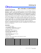
W9825G6CH 4M × 4 BANKS × 16 BIT SDRAM GENERAL DESCRIPTION W9825G6CH is a high-speed synchronous dynamic random access memory (SDRAM), organized as 4M words × 4 banks × 16 bits. Using pipelined architecture and 0.13 µm process technology, W9825G6CH delivers a data bandwidth of up to 166M words per second (-6). To fully comply with the personal computer industrial standard, W9825G6CH is sorted into two speed grades: -6, -7 and -75.
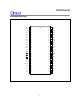
W9825G6CH PIN CONFIGURATION VCC 1 54 V SS DQ0 2 53 DQ15 V C CQ 3 52 V SS Q DQ1 4 51 DQ14 DQ2 5 50 DQ13 V SS Q 6 49 V C CQ DQ3 7 48 DQ12 8 47 DQ11 V C CQ 9 46 V SS Q DQ5 10 45 DQ10 DQ6 11 44 DQ9 V SS Q 12 43 V C CQ DQ7 13 42 DQ8 VCC 14 41 V SS LDQM 15 40 NC WE 16 39 UDQM CAS 17 38 CLK RAS 18 37 CKE DQ4 CS 19 36 A12 BS0 20 35 A11 BS1 21 34 A9 A10/AP 22 33 A8 A0 23 32 A7 A1 24 31 A6 A2 25 30 A5 A3 26 29 A4
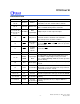
W9825G6CH PIN DESCRIPTION PIN NO. PIN NAME FUNCTION 23−26, 22, 29−36 A0−A12 Address 20, 21 BS0, BS1 Bank Select DESCRIPTION Multiplexed pins for row and column address. Row address: A0−A12. Column address: A0−A8. Select bank to activate during row address latch time, or bank to read/write during address latch time. 2, 4, 5, 7, 8, 10, 11, 13, 42, 44, Data Multiplexed pins for data output and input.
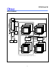
W9825G6CH BLOCK DIAGRAM CLK CLOCK BUFFER CKE CS CONTROL RAS GENERATOR SIGNAL COMMAND CAS DECODER COLUMN DECODER COLUMN DECODER A10 BANK #0 MODE REGISTER A0 CELL ARRAY BANK #1 SENSE AMPLIFIER SENSE AMPLIFIER ADDRESS BUFFER DQ0 DATA CONTROL DQ BUFFER CIRCUIT DQ15 COLUMN COUNTER LDQM UDQM COLUMN DECODER CELL ARRAY BANK #2 SENSE AMPLIFIER Note: The cell array configuration is 8192 * 512 * 16.
W9825G6CH ABSOLUTE MAXIMUM RATINGS PARAMETER SYMBOL RATING UNIT NOTES Input, Output Voltage VIN, VOUT -0.3 − VCC + 0.3 V 1 Supply Voltage VCC, VCCQ -0.3 − 4.
W9825G6CH AC CHARACTERISTICS AND OPERATING CONDITION (Vcc = 3.3V ± 0.3V, Ta = 0 to 70°C for –6/-7/-75/75L, Ta=-40 to 85°C for 75I ; Notes: 5, 6, 7, 8) PARAMETER SYM. Ref/Active to Ref/Active Command Period Active to precharge Command Period Active to Read/Write Command Delay Time Read/Write(a) to Read/Write(b) Command Period Precharge to Active Command Period Active(a) to Active(b) Command Period Write Recovery Time CL* = 2 CL* = 2 Access Time from CLK CL* = 2 MIN. MAX. MAX.
W9825G6CH PARAMETER SYM. UNIT -6 MIN. MAX. Ref/Active to Ref/Active Command Period tRC 60 Active to precharge Command Period tRAS tRCD 42 18 nS tCCD 1 tCK tRP 18 nS Active(a) to Active(b) Command Period tRRD 12 nS Write Recovery Time tWR 2 tCK 2 tCK Active to Read/Write Command Delay Time Read/Write(a) to Read/Write(b) Command Period Precharge to Active Command Period CL* = 2 CL* = 3 CLK Cycle Time CL* = 2 tCK CL* = 3 CLK High Level Width nS 100000 nS 7.
W9825G6CH DC CHARACTERISTICS (VCC = 3.3V ± 0.3V, Ta = 0 to 70°C for –6/-7/-75/75L, Ta=-40 to 85°C for 75I) PARAMETER Operating Current SYM. -6 -7 -75/75L/75I MAX. MAX. UNIT NOTES 1 Bank Operation ICC1 90 80 75 3 CKE = VIH ICC2 50 40 35 3 CKE = VIL (Power ICC2P 2 2 2 3 CKE = VIH ICC2S 10 10 10 CKE = VIL (Power ICC2PS 2 2 2 CKE = VIH ICC3 70 60 55 CKE = VIL (Power ICC3P 10 10 10 ICC4 110 100 95 3, 4 ICC5 180 170 160 3 3 3 3 - 1 tCK = min.
W9825G6CH Notes: 1. Operation exceeds "ABSOLUTE MAXIMUM RATING" may cause permanent damage to the devices. 2. All voltages are referenced to VSS 3. These parameters depend on the cycle rate and listed values are measured at a cycle rate with the minimum values of tCK and tRC. 4. These parameters depend on the output loading conditions. Specified values are obtained with output open. 5. Power up sequence is further described in the "Functional Description" section. 6.
W9825G6CH OPERATION MODE Fully synchronous operations are performed to latch the commands at the positive edges of CLK. Table 1 shows the truth table for the operation commands.
W9825G6CH FUNCTIONAL DESCRIPTION Power Up and Initialization The default power up state of the mode register is unspecified. The following power up and initialization sequence need to be followed to guarantee the device being preconditioned to each user specific needs. During power up, all Vcc and VccQ pins must be ramp up simultaneously to the specified voltage when the input signals are held in the "NOP" state. The power up voltage must not exceed Vcc +0.3V on any of the input pins or Vcc supplies.
W9825G6CH Burst Read Command The Burst Read command is initiated by applying logic low level to CS and CAS while holding RAS and WE high at the rising edge of the clock. The address inputs determine the starting column address for the burst. The Mode Register sets type of burst (sequential or interleave) and the burst length (1, 2, 4, 8, full page) during the Mode Register Set Up cycle. Table 2 and 3 in the next page explain the address sequence of interleave mode and sequential mode.
W9825G6CH Addressing Sequence of Sequential Mode A column access is performed by increasing the address from the column address which is input to the device. The disturb address is varied by the Burst Length as shown in Table 2.
W9825G6CH Auto-precharge Command If A10 is set to high when the Read or Write Command is issued, then the auto-precharge function is entered. During auto-precharge, a Read Command will execute as normal with the exception that the active bank will begin to precharge automatically before all burst read cycles have been completed. Regardless of burst length, it will begin a certain number of clocks prior to the end of the scheduled burst cycle. The number of clocks is determined by CAS latency.
W9825G6CH The Power Down mode is exited by bringing CKE high. When CKE goes high, a No Operation Command is required on the next rising clock edge, depending on tCK. The input buffers need to be enabled with CKE held high for a period equal to tCKS (min) + tCK (min). No Operation Command The No Operation Command should be used in cases when the SDRAM is in a idle or a wait state to prevent the SDRAM from registering any unwanted commands between operations.
W9825G6CH TIMING WAVEFORMS Command Input Timing Command Input Timing tCL tCK tCH VIH CLK VIL tT tCMS tCMH tCMS tCMH tCMS tCMH tCMS tCMH tAS tAH tCMH CS RAS CAS WE A0-A12 BS0, 1 tCKS tCKH tCKS tCKH tCKS CKE - 16 - tCKH tT tCMS
W9825G6CH Timing Waveforms, continued Read Timing Read CAS Latency CLK CS RAS CAS WE A0 - A12 BS0, 1 tAC tAC tLZ tHZ tOH tOH Valid Data-Out DQ Read Command Valid Data-Out Burst Length - 17 - Publication Release Date: Oct.
W9825G6CH Timing Waveforms, continued Control Timing of Input/Output Data Input Data (Word Mask) CLK t CMS t CMH tCMH t CMS DQM t DS t DH tDS Valid Data-in DQ0 -15 tDH t DS Valid Data-in t DH t DS Valid Data-in t DH Valid Data-in (Clock Mask) CLK t CKH t CKS tDH t DS t CKH t CKS CKE t DS DQ0 -15 Valid Data-in t DH t DS Valid Data-in t DH tDS Valid Data-in t DH Valid Data-in Output Data (Output Enable) CLK tCMH t CMS t CMS tCMH DQM t AC t OH t OH tLZ t OH Valid Data-O
W9825G6CH Timing Waveforms, continued Mode Register Set Cycle tRSC CLK tCMS tCMH tCMS tCMH tCMS tCMH tCMS tCMH CS RAS CAS WE tAS A0-A12 BS0,1 tAH Register set data A0 A1 Burst Length A2 A3 Addressing Mode A4 A5 CAS Latency A2 0 0 0 0 1 1 1 1 A6 A7 A0 "0" (Test Mode) A8 "0" Reserved A9 A0 WriteA0 Mode A10 "0" A11 A0 "0" A12 "0" BS0 A0 "0" BS1 A0 "0" A0 Reserved A6 0 0 0 0 1 A0 A1 A0 A0 0 A0 0 A0 1 A0 1 A0 0 A0 0 A0 1 A0 1 A3 A0 A0 0 A0 1 A5 A0 A0 0 A0 0 A0 1 A0 1 A
W9825G6CH OPERATING TIMING EXAMPLE Interleaved Bank Read (Burst Length = 4, CAS Latency = 3) (CLK = 100 MHz) 1 0 2 3 4 6 5 7 8 9 10 11 12 13 14 15 16 17 18 19 20 21 22 23 CLK CS tRC tRC tRC tRC RAS tRAS tRP tRAS tRAS tRP tRP tRAS CAS WE BS0 BS1 tRCD A10 RAa A0-A9, A11,12 RAa tRCD tRCD RBb CBx RBb CAw tRCD RAc RBd RAc CAy RAe RBd CBz RAe DQM CKE aw0 tRRD Bank #0 Active Bank #1 tAC tAC tAC DQ aw1 aw2 aw3 bx0 Precharge Active bx2 bx3 Activ
W9825G6CH Operating Timing Example, continued Interleaved Bank Read (Burst Length = 4, CAS Latency = 3, Autoprecharge) (CLK = 100 MHz) 0 1 2 3 4 6 5 7 8 9 10 11 12 13 14 15 16 17 18 19 20 21 22 23 CLK CS tRC tRC tRC tRC RAS tRAS tRP tRAS tRAS tRP tRP tRAS CAS WE BS0 BS1 tRCD A10 RAa A0-A9, A11,12 RAa tRCD tRCD RBb CAw tRCD CBx RBb RAe RBd RAc CAy RAc CBz RBd RAe DQM CKE tAC DQ tRRD Bank #0 Active Bank #1 aw1 aw2 aw3 bx0 Active bx1 bx2 bx3 tA
W9825G6CH Operating Timing Example, continued Interleaved Bank Read (Burst Length = 8, CAS Latency = 3) (CLK = 100 MHz) 0 1 2 3 4 5 6 7 8 9 10 11 12 13 14 15 16 17 18 19 20 21 CLK CS tRC tRC tRC RAS tRAS tRP tRAS tRP tRAS tRP CAS WE BS0 BS1 tRCD A10 RAa A0-A9, A11,12 RAa tRCD tRCD RAc RBb CAx RBb CBy RAc CAz DQM CKE tAC DQ tAC ax0 ax1 tRRD Bank #0 Active Bank #1 ax2 ax3 ax4 ax5 by0 by1 by4 by5 by6 by7 tRRD Read Precharge ax6 tAC Precharge Acti
W9825G6CH Operating Timing Example, continued Interleaved Bank Read (Burst Length = 8, CAS Latency = 3, Autoprecharge) (CLK = 100 MHz) 0 1 2 3 4 5 6 7 8 9 10 11 12 13 14 15 16 17 18 19 20 21 22 23 CLK tRC CS tRC RAS tRAS tRP tRAS tRAS tRP CAS WE BS0 BS1 tRCD tRCD tRCD A10 A0-A9, A11,12 RBb RAa RAa CAx RAc RBb CAz RAc CBy DQM CKE tCAC tCAC DQ ax0 ax1 ax2 tRRD Bank #0 Active ax4 ax5 ax6 ax7 by0 by1 by4 by5 by6 CZ0 tRRD AP* Read Active Bank
W9825G6CH Operating Timing Example, continued Interleaved Bank Write (Burst Length = 8) (CLK = 100 MHz) 1 0 2 3 4 5 6 7 8 9 10 11 12 13 14 15 16 17 18 19 20 21 22 23 CLK CS tRC RAS tRAS tRAS tRP tRP tRAS CAS tRCD tRCD tRCD WE BS0 BS1 A10 RAa A0-A9, A11,12 RAa RBb CAx RAc RBb CBy RAc CAz DQM CKE DQ ax0 ax1 ax4 ax5 ax6 ax7 by0 by1 tRRD Bank #0 Active Precharge Write Write Bank #2 Bank #3 by3 by4 by5 by6 by7 CZ0 CZ1 CZ2 tRRD Active Bank
W9825G6CH Operating Timing Example, continued Interleaved Bank Write (Burst Length = 8, Autoprecharge) (CLK = 100 MHz) 0 1 2 3 4 5 6 7 8 9 10 11 12 13 14 15 16 17 18 19 20 21 22 23 CLK CS tRC RAS tRP t RAS tRAS tRAS tRP CAS WE BS0 BS1 tRCD tRCD A10 RAa A0-A9, A11 RAa tRCD RBb CAx RAb CBy RBb CAz RAc DQM CKE DQ ax0 ax1 ax4 ax5 ax6 ax7 by0 by1 tRRD Bank #0 Active by3 by4 by5 by6 by7 CZ0 CZ1 CZ2 tRRD AP* Write Active Bank #1 by2 Write Ac
W9825G6CH Operating Timing Example, continued Page Mode Read (Burst Length = 4, CAS Latency = 3) (CLK = 100 MHz) 0 1 2 3 4 5 6 7 8 9 10 11 12 13 14 15 16 17 18 19 20 21 22 CLK tCCD t CCD tCCD CS t RAS tRP tRAS tRP RAS CAS WE BS0 BS1 tRCD A10 A0-A9, A11,12 tRCD RAa RBb RAa RBb CAI CBx CAy CAm CBz DQM CKE tAC DQ tAC tAC a0 a1 a2 a3 bx0 bx1 Ay0 tAC Ay1 Ay2 t AC am0 am1 am2 bz0 bz1 t RRD Bank #0 Active Read Active Bank #1 Read Read Read Pre
W9825G6CH Operating Timing Example, continued Page Mode Read/Write (Burst Length = 8, CAS Latency = 3) (CLK = 100 MHz) 0 1 2 3 4 5 6 7 8 9 10 11 12 13 14 15 16 17 18 19 20 21 22 23 CLK CS tRAS tRP RAS CAS WE BS0 BS1 tRCD A10 RAa A0-A9, A11,12 RAa CAx CAy DQM CKE tAC DQ tWR ax0 Q Q Bank #0 Active ax1 ax2 Q Q ax3 Q ax5 ax4 Q Read ay1 ay0 D D Write D ay2 ay4 ay3 D D Precharge Bank #1 Bank #2 Bank #3 Idle - 27 - Publication Release Date: Oct.
W9825G6CH Operating Timing Example, continued Auto Precharge Read (Burst Length = 4, CAS Latency = 3) (CLK = 100 MHz) 0 1 2 3 4 5 6 7 8 9 10 11 12 13 14 15 16 17 18 19 20 21 22 CLK CS tRC tRC RAS tRAS tRP tRAS tRP CAS WE BS0 BS1 tRCD A10 RAa A0-A9, A11,12 RAa tRCD RAb CAw RAb CAx DQM CKE tAC DQ Bank #0 tAC aw0 Active Read aw1 AP* aw2 aw3 bx0 Active Read Bank #1 Bank #2 Idle Bank #3 * AP is the internal precharge start timing - 28 - bx1 AP* bx2 bx3
W9825G6CH Operating Timing Example, continued Auto Precharge Write (Burst Length = 4) (CLK = 100 MHz) CLK 0 1 2 3 4 5 6 7 8 9 10 11 12 13 14 15 16 17 18 19 20 21 22 23 CS tRC tRC RAS tRAS tRP tRAS tRP CAS WE BS0 BS1 tRCD tRCD A10 RAa A0-A9, A11 RAa RAc RAb CAw RAb CAx RAc DQM CKE DQ Bank #0 aw0 Active aw1 Write aw2 bx0 aw3 AP* Active bx1 Write bx2 bx3 AP* Active Bank #1 Bank #2 Idle Bank #3 * AP is the internal precharge start timing - 29 - P
W9825G6CH Operating Timing Example, continued Auto Refresh Cycle (CLK = 100 MHz) 0 1 2 3 4 5 6 7 8 9 10 11 12 13 14 15 16 17 18 19 20 CLK t RP t RC t RC CS RAS CAS WE BS0,1 A10 A0-A9, A11,12 DQM CKE DQ All Banks Prechage Auto Refresh Auto Refresh (Arbitrary Cycle) - 30 - 21 22 23
W9825G6CH Operating Timing Example, continued Self Refresh Cycle (CLK = 100 MHz) 0 1 2 3 4 5 6 7 8 9 10 11 12 13 14 15 16 17 18 19 20 21 22 23 CLK CS tRP RAS CAS WE BS0,1 A10 A0-A9, A11,12 DQM t CKS tCKS tSB CKE tCKS DQ tRC Self Refresh Cycle All Banks Precharge No Operation Cycle Self Refresh Entry Arbitrary Cycle - 31 - Publication Release Date: Oct.
W9825G6CH Operating Timing Example, continued Burst Read and Single Write (Burst Length = 4, CAS Latency = 3) (CLK = 100 MHz) 0 1 2 3 4 5 6 7 8 9 10 11 12 13 14 15 16 17 18 19 20 21 CLK CS RAS CAS tRCD WE BS0 BS1 A10 RBa A0-A9, A11,12 RBa CBv CBw CBx CBy CBz DQM CKE t AC DQ tAC av0 Q Bank #0 Active Bank #1 Bank #2 Bank #3 av1 Q av2 av3 aw0 ax0 ay0 az0 az1 az2 az3 Q Q D D D Q Q Q Q Read Single Write Idle - 32 - Read 22 23
W9825G6CH Operating Timing Example, continued PowerDown Mode (CLK = 100 MHz) 0 1 2 3 4 5 6 7 8 9 10 11 12 13 14 15 16 17 18 19 20 21 22 23 CLK CS RAS CAS WE BS A10 RAa A0-A9 A11,12 RAa RAa CAa RAa CAx DQM tSB tSB CKE tCKS tCKS tCKS DQ ax0 Active ax1 ax2 NOP Read tCKS ax3 Precharge NOPActive Precharge Standby Power Down mode Active Standby Power Down mode Note: The PowerDown Mode is entered by asserting CKE "low".
W9825G6CH Operating Timing Example, continued Autoprecharge Timing (Read Cycle) 0 1 Read AP 2 3 4 5 6 7 8 9 10 11 (1) CAS Latency=2 ( a ) burst length = 1 Command DQ Act tRP Q0 ( b ) burst length = 2 Command Read AP Act tRP DQ Q0 Q1 ( c ) burst length = 4 Command Read AP Act tRP DQ Q0 Q1 Q2 Q3 Q0 Q1 Q2 Q3 ( d ) burst length = 8 Command Read AP DQ Q4 Q5 Q6 Act tRP Q7 (2) CAS Latency=3 ( a ) burst length = 1 Command Read AP Act tRP Q0 DQ ( b ) burst leng
W9825G6CH Operating Timing Example, continued Autoprecharge Timing (Write Cycle) 0 1 2 3 4 5 6 7 8 9 10 11 12 (1) CAS Latency = 2 (a) burst length = 1 Command Write AP tWR DQ Act tRP D0 (b) burst length = 2 Command Write AP Act tWR DQ D0 tRP D1 (c) burst length = 4 Command AP Write DQ D0 D1 D2 Act tRP tWR D3 (d) burst length = 8 Command Write AP tWR DQ D0 D1 D2 D3 D4 D5 D6 Act tRP D7 (2) CAS Latency = 3 (a) burst length = 1 Command Write AP Act tWR D
W9825G6CH Operating Timing Example, continued Timing Chart of Read to Write Cycle In the case of Burst Length = 4 (1) CAS Latency=2 0 1 2 3 4 5 D1 D2 D3 D0 D1 D2 D1 D2 D3 D1 D2 6 7 8 9 10 11 9 10 11 Read Write ( a ) Command DQM DQ D0 Read ( b ) Command Write DQM DQ D3 (2) CAS Latency=3 Read Write ( a ) Command DQM D0 DQ Read ( b ) Command Write DQM D0 DQ D3 Note: The Output data must be masked by DQM to avoid I/O conflict Timing Chart of Write to Read Cycl
W9825G6CH Timing Chart of Burst Stop Cycle (Burst Stop Command) 0 1 2 3 4 5 6 7 8 9 10 11 (1) Read cycle ( a ) CAS latency =2 Command Read BST Q0 DQ Q1 Q2 Q0 Q1 Q3 Q4 ( b )CAS latency = 3 Command Read BST DQ Q2 Q3 Q4 (2) Write cycle Command DQ Write Q0 BST Q1 Q2 Note: Q3 BST Q4 represents the Burst stop command Timing Chart of Burst Stop Cycle (Precharge Command) - 37 - Publication Release Date: Oct.
W9825G6CH 0 1 2 3 4 5 6 7 (1) Read cycle (a) CAS latency =2 Command Read PRCG DQ (b) CAS latency =3 Command Q0 Q1 Q2 Read Q3 Q4 PRCG DQ Q0 Q1 Q2 Q3 (2) Write cycle (a) CAS latency =2 PRCG Write Command tWR DQM DQ (b) CAS latency =3 Command Q0 Q1 Q2 Q3 Q4 PRCG Write tWR DQM DQ Q0 Q1 Q2 Q3 Q4 - 38 - Q4 8 9 10 11
W9825G6CH Operating Timing Example, continued CKE/DQM Input Timing (Write Cycle) CLK cycle No. 1 2 3 D1 D2 D3 4 5 6 7 External CLK Internal CKE DQM DQ D5 DQM MASK D6 CKE MASK (1) CLK cycle No. 1 2 3 D1 D2 D3 4 5 6 7 External CLK Internal CKE DQM DQ D5 DQM MASK D6 CKE MASK (2) CLK cycle No. 1 2 3 D1 D2 D3 4 5 6 7 External CLK Internal CKE DQM DQ D4 D5 D6 CKE MASK (3) - 39 - Publication Release Date: Oct.
W9825G6CH Operating Timing Example, continued CKE/DQM Input Timing (Read Cycle) CLK cycle No. 1 2 3 4 Q 1 Q 2 Q 3 Q 4 5 6 7 External CLK Internal CKE DQM DQ Open Open Q 6 (1) CLK cycle No. 1 2 3 Q 1 Q 2 Q 3 4 5 6 7 External CLK Internal CKE DQM DQ Q 4 Open Q 6 (2) CLK cycle No.
W9825G6CH Operating Timing Example, continued Self Refresh/Power Down Mode Exit Timing Asynchronous Control Input Buffer turn on time ( Power down mode exit time ) is specified by tCKS(min) + tCK(min) A ) tCK < tCKS(min)+tCK(min) tCK CLK CKE tCKS(min)+tCK(min) NOP Command Command Input Buffer Enable B) tCK >= tCKS(min) + tCK (min) tCK CLK tCKS(min)+tCK(min) CKE Command Command Input Buffer Enable Note ) All Input Buffer(Include CLK Buffer) are turned off in the Power Down mode and Self Refre
W9825G6CH PACKAGE DIMENSION 54L TSOP (II)-400 mil 54 28 HE E 1 27 e b C D L A2 A1 ZD Y SEATING PLANE Controlling Dimension: Millimeters DIMENSION (MM) DIMENSION (INCH) SYM. MIN. NOM. A A1 A2 b 0.05 0.10 MAX. 1.20 0.15 MIN. 0.002 1.00 0.24 c 0.32 NOM. 0.004 MAX. 0.047 0.006 0.039 0.40 0.009 0.012 0.006 0.016 0.15 D 22.12 22.22 22.62 0.871 0.875 0.905 E 10.06 10.16 10.26 0.396 0.400 0.404 HE e 11.56 11.76 11.96 0.455 0.463 0.471 L 0.40 L1 0.80 0.50 0.
W9825G6CH 11. REVERSION HISTORY REVERSION A1 DATE PAGE March, 2003 - A2 Headquarters DESCRIPTION Preliminary datasheet. Oct, 2003 Add –6 speed grade. 1 Oct, 2004 Add the PB free description. Winbond Electronics (H.K.) Ltd. Unit 9-15, 22F, Millennium City, No. 4, Creation Rd. III, No. 378 Kwun Tong Rd; Science-Based Industrial Park, Kowloon, Hong Kong Hsinchu, Taiwan TEL: 852-27513100 TEL: 886-3-5770066 FAX: 852-27552064 FAX: 886-3-5796096 http://www.winbond.com.