
Datasheet


FM24C64B
Rev. 1.3
Feb. 2011 10 of 12
AC Test Conditions Equivalent AC Load Circuit
Input Pulse Levels 0.1 V
DD
to 0.9 V
DD
Input rise and fall times 10 ns
Input and output timing levels 0.5 V
DD
Diagram Notes
All start and stop timing parameters apply to both read and write
cycles. Clock specifications are identical for read and write cycles.
Write timing parameters apply to slave address, word address, and
write data bits. Functional relationships are illustrated in the relevant
data sheet sections. These diagrams illustrate the timing parameters
only.
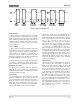
Read Bus Timing
t
SU:SDA
Start
t
R
t
F
Stop Start
t
BUF
t
HIGH
1/fSCL
t
LOW
t
SP
t
SP
Acknowledge
t
HD:DAT
t
SU:DAT
t
AA
t
DH
SCL
SDA
Write Bus Timing
t
SU:STO
Start
Stop Start Acknowledge
t
AA
t
HD:DAT
t
HD:STA
t
SU:DAT
SCL
SDA
Data Retention
Symbol Parameter Min Max Units Notes
T
DR
@
+85ºC 10 - Years
@
+80ºC 19 - Years
@
+75ºC 38 - Years
5.5V
Output
1700
Ω
100 pF