
User's Manual

Rev2.0 (7/28) Confidential and Proprietary ©2012-2014 by Rayson Corporation, not for distribution. Page 4 of 13
Confidential A Confidential Information contained herein is covered under Non-Disclosure Agreement (NDA).
Preliminary datasheet, Rayson Corporation reserves right to modify without notification
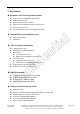
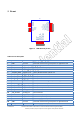
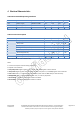
3 Pin out
Figure 1 PCB Antenna pin out
Table 1 Pin out description
PIN
NAME FUNCTION DESCRIPTION
1 GND Ground Should be connected to ground plane on application PCB
2 /RSTN Digital Input Hardware reset, active low.
3 P2.3/SDA Digital in/out GPIO / I2C data with pull-up
4 P2.4/SCL Digital in/out GPIO / I2C clock
5 P1.0/SPI_MISO Digital in/out GPIO / SPI data master in/slave out
6 P1.1/SPI_MOSI Digital in/out GPIO / SPI data master out/slave in
7 P1.2/SPI_CS Digital in/out GPIO / SPI chip select
8 P1.3/SPI_CLK Digital in/out GPIO / SPI clock
9 GND Ground Should be connected to ground plane on application PCB
10 P1.7/UART_RX
Digital input
GPIO / UART RX data input
11 P0.0/UART_TX Digital output GPIO / UART TX data output
12 P0.3/INT0 Digital in GPIO / Interrupt
13 32K_CLOCK1 Analog in Not connected
14 32K_CLOCK2 Analog out Not connected
15 SWDIO Digital in/out SWD data with pull-up
16 SWCLK Digital in SWD clock input with pull-up
17 VCC Power Power supply (2.4~3.6V)
18 GND Ground Should be connected to ground plane on application PCB
19 VDD_IDC Power Power supply (2.4~3.6V)
U4
GND
1
/RSTN
2
P2.3_I2C-SDA
3
P2.4_I2C-SCL
4
P1.0_SPI1-MISO
5
P1.1_SPI1-MOSI
6
P1.2_SPI1-CS
7
P1.3_SPI1-CLK
8
GND
9
GND
18
VDD_IDC
19
P3.0_ADC-
20
P3.1_ADC+
21
GND
22
GND
23
GND
24
GND
25
SWCLK
16
XTAL_32K_IN
14
P0.3_INT0
12
SWDIO
15
EXT_VCC
17
P0.0_UART0-TX
11
P1.7_UART0-RX
10
XTAL_32K_OUT
13