
Specifications


TC35 / TC37 Hardware Interface Description
TC35_37_HD_02_V03.10 - Released Page 82 of 92 21.12.2001
Note: With regard to acoustic shock, the cellular application must be designed to avoid
sending false AT commands that might increase amplification, e.g. for a high
sensitive earpiece. A protection circuit should be implemented in the cellular
application.
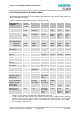
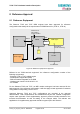
6.5.3 Voiceband receive path
The values specified below were tested to 1kHz and 0dB gain stage, unless otherwise
stated.
gs = 0dB means audio mode = 5 for EPP1 to EPN1 and 6 for EPP2 to EPN2, inBbcGain= 0,
inCalibrate = 32767, outBbcGain = 0, OutCalibrate = 16384, sideTone = 0.
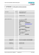
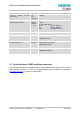
Table 36: Voiceband receive path
Parameter Min Typ Max Unit Test condition / remark
Differential output
voltage (peak to peak)
3.33 3.7 4.07 V from EPPx to EPNx
gs = 0dB @ 3.14 dBm0
Differential output gain
settings (gs) at 6dB
stages (outBbcGain)
-18 0 dB
fine scaling by DSP
(outCalibrate)
-# 0 dB
Output differential
DC offset
100 mV gs = 0dB, outBbcGain = 0 and -6dB
Differential output
resistance
13 15 " from EPPx to EPNx
Absolute gain accuracy 0.8 dB Variation due to change in VDD,
temperature and life time
Attenuation distortion 1 dB for 300...3900Hz,
@ EPPx/EPNx (333Hz) /
@ EPPx/EPNx (3.66kHz)
Out-of-band
discrimination
60 dB for f > 4kHz with in-band test signal
@ 1kHz and 1kHz RBW
gs = gain setting