
User's Manual
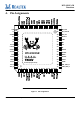


RTL8191E-GR
Datasheet
Wireless LAN Network Interface Controller 11 Rev.0.4
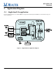
5.6.
Clock and Other Pins
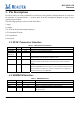
Table 6. Clock and Other Pins
Symbol Type Pin No Description
XI I 25 40MHz OSC Input.
Input of 40MHz Crystal clock reference.
XO O 26 Output of 40MHz Crystal clock reference.
ISOLATIONn I 48 This pin can externally shutdown 8191SE without extra power switch. This pin can
also support WLAN Radio off function with host interface remaining connected.
VAUXEN/EESK I 62 Weakly pull high at power on to indicate the presence of the auxiliary power on the
mainboard. Otherwise, this is for EEPROM autoload.
GPIO0/WLAN_
ACT
I/O 29 There are 8 General Purpose Input/Output pins. Some are used for power-on latch and
Bluetooth coexistence, and also EEPROM purposes.
The WLAN_ACT signal indicates when WLAN is either transmitting or receiving in
the 2.4GHz ISM band.
GPIO1/WLAN_R
X
I/O 30 Wireless LAN RX activity indicator.
GPIO2/BT_STAT
E
I/O 31 The BTSTAT signal indicates when normal Bluetooth packets are being transmitted or
received.
GPIO3/BT_PRI I/O 32 Left not connected if the EEPROM in use is 93C46.
The BTPRI signal indicates when a high priority Bluetooth packet is being transmitted
or received.
GPIO4 I/O 56 GPIO4.
GPIO5 I/O 57 GPIO5.
GPIO6/EEDO I/O 60 EEPROM interface EEDO signal.
GPIO7/EEDI I/O 61 EEPROM interface EEDI signal.
6. Electrical and Thermal Characteristics
6.1.
Temperature Limit Ratings
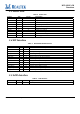
Table 8. Temperature Limit Ratings
Parameter Minimum Maximum Units
Storage Temperature -55 +125 ° C
Ambient Operating Temperature 0 70 ° C
Junction Temperature 0 125 ° C
6.2.
DC Characteristics
Below is a description of the general DC specifications for the RTL8191SE.
Table 9. DC Characteristics
Symbol Parameter Conditions Minimum Typical Maximum Units
DVDD33 3.3V I/O Supply Voltage 3.135 3.3 3.465 V