
Product data
17
32176 Group
Mitsubishi Microcomputers
SINGLE-CHIP 32-BIT CMOS MICROCOMPUTER
Under Development
Jan. 30, 2003 Rev.1.4
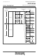
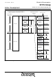
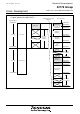
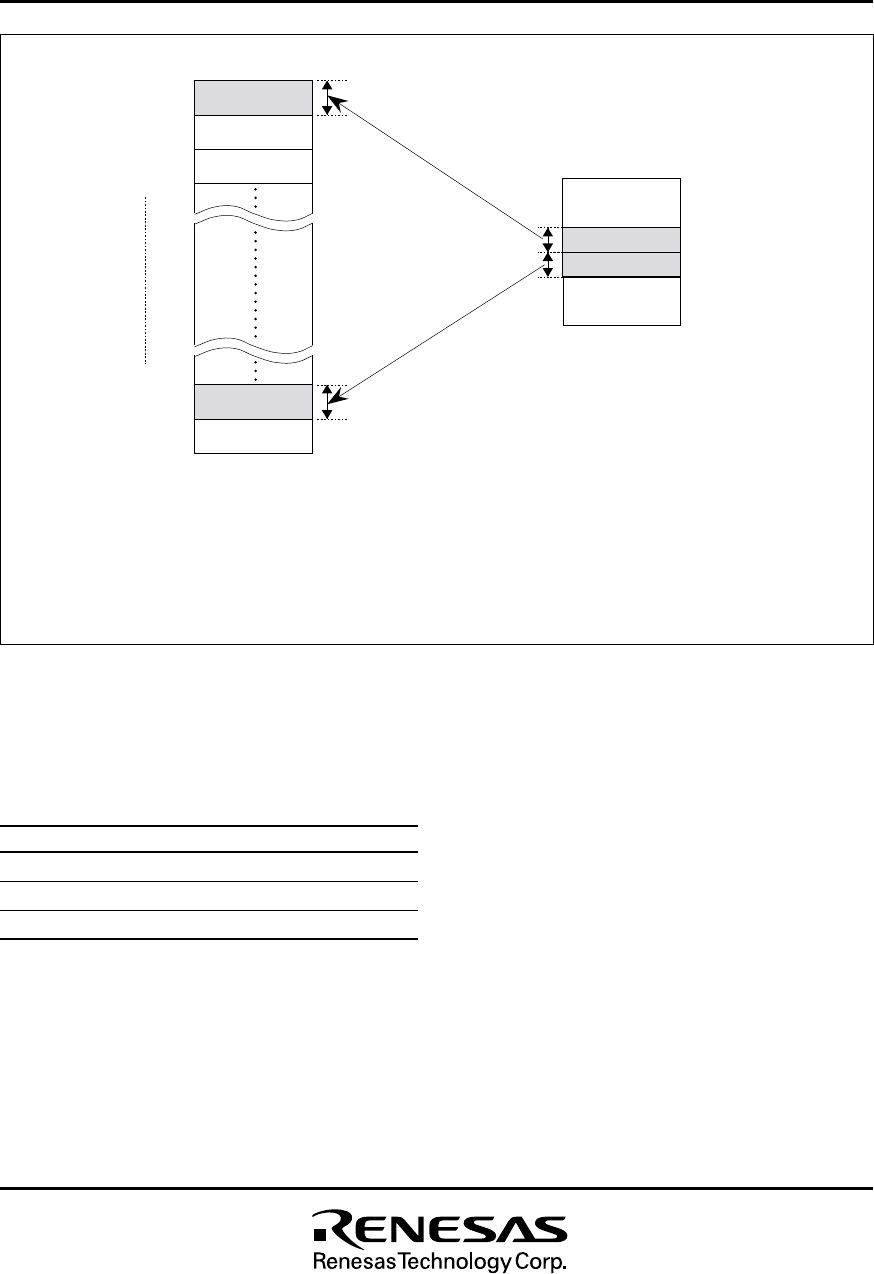
H'0000 0000
H'0000 1000
< Internal RAM >
H'0080 4000
H'0080 5FFF
S bank 0
(4K bytes)
H'0000 2000
8K bytes
H'0000 0FFF
H'0000 1FFF
H'0000 2FFF
H'0007 F000
H'0007 FFFF
H'0007 E000
H'0007 EFFF
4K bytes
4K bytes
H'0080 6000
H'0080 7000
8K bytes
H'0080 8000
H'0080 9FFF
< Internal flash >
S bank 1
(4K bytes)
S bank 2
(4K bytes)
S bank 126
(4K bytes)
S bank 127
(4K bytes)
Figure 9. Virtual-Flash Emulation Areas of the M32176F4VFP/M32176F4TFP (Replaced in Units of 4K bytes)
Notes: • If the same bank area is set in multiple virtual-flash bank registers and the virtual-flash emulation enable bit is enabled, the
corresponding internal RAM area is assigned to either bank register according to the priority FELBANK0 > FESBANK0 >
FESBANK1 > FELBANK1.
• When access is made to the 4K bytes area (S bank) specified with virtual-flash bank register 0 and 1, the internal RAM area
is accessed. During virtual-flash emulation mode, RAM data can read and written to and from both the internal RAM area and
the virtual-flash setup area.
Virtual-Flash Emulation Areas of M32176F4VFP/M32176F4TFP,
M32176F3VFP/M32176F3TFP, and M32176F2VFP/M32176F2TFP
are shown as follows.
Table 8. Virtual-Flash Emulation Areas
Type Name Virtual-Flash Emulation Areas
M32176F4VFP/M32176F4TFP H’0000 0000-H’0007 FFFF
M32176F3VFP/M32176F3TFP H’0000 0000-H’0005 FFFF
M32176F2VFP/M32176F2TFP H’0000 0000-H’0003 FFFF