
Product data


7
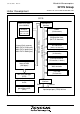
32176 Group
Mitsubishi Microcomputers
SINGLE-CHIP 32-BIT CMOS MICROCOMPUTER
Under Development
Jan. 30, 2003 Rev.1.4
Table 4. Description of Pin Function (1/4)
Type Pin Name Input/Output Function
Power VCCE Power supply - Power supply (5.0V ± 0.5V or 3.3V ± 0.3V).
EXCVCC Internal power - External capacitance connecting pin.
supply
VDDE RAM power supply - Internal RAM backup power supply (5.0V ± 0.5V or 3.3V ± 0.3V).
EXCVDD Internal power - Backup power supply for the internal RAM, external capacitance con
supply of RAM necting pin.
VSS Ground - Connect all VSS pins to ground (GND).
Clock XIN Clock input Input Clock input/output pins. These pins contain a PLL-based
XOUT Clock output Output frequency multiply-by-4, so input the clock whose frequency is quarter
the operating frequency. (XIN input = 10 MHz when CPU clock operates
at 40 MHz)
BCLK System clock Output Outputs a clock twice the externally sourced clock frequency, XIN
(when the internal CPU memory clock is 80 MHz, BCLK output = 20
MHz).
Use this output when external sync design is desired.
EXCOSC Internal power - External capacitance connecting pin.
-VCC supply
OSC-VSS Ground - Connect OSC-VSS to ground.
Reset RESET# Reset Input This pin resets the internal circuits.
Mode MOD0, Mode Input These pins set an operation mode.
MOD1 MOD0 MOD1 Mode
0 0 Single-chip mode
0 1 Expanded external mode
1 0 Processor mode
(Boot mode) (Note 1)
1 1 (Reserved)
MOD2 Mode Input Please be sure to connect MOD2 to ground (GND).
Flash-only FP Flash Protect Input This pin protects the flash memory against E/W in hardware.
Address A12-A30 Address Output 19 lines of address bus (A12-A30) are provided to accommodate two
bus bus channels of 1 MB memory space (max.) connected external to the
chip. A31 is not output.
Data bus DB0-DB15 Data bus Input/output This is a 16-bit data bus connecting to an external device. During write
cycle, the microcomputer outputs BHW# or BLW# to indicate the valid
byte write position of the 16-bit data bus. During read cycle, the micro
computer always reads the full 16-bit data bus. Transferred to the internal
circuit of the M32R, however, is the data at only the valid byte position.
Note 1: In boot mode, the FP pin must be at the high level.