
Datasheet


Section 28 Electrical Characteristics
Rev. 2.00 Sep. 28, 2009 Page 973 of 994
REJ09B0452-0200
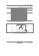
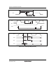
FSICK
FSICK
FSISS
FSIDO
FSIDI
t
TXD
t
SSL
t
CKH
t
CKL
t
CYC
t
SSH
t
RXH
t
RXS
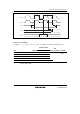
Figure 28.22 FSI Input/Output Timing
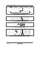
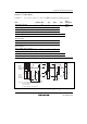
Table 28.8 PS2 Timing
Conditions: V
CC
= 3.0 V to 3.6 V, V
SS
= 0 V, φ = 8 MHz to maximum operating frequency
Standard Value
Item Symbol Min. Typ. Max. Unit
Test
Conditions Remarks
KCLK, KD output fall time t
KBF
⎯ ⎯ 250 ns
KCLK, KD input data hold time t
KBIH
150 ⎯ ⎯
KCLK, KD input data setup time t
KBIS
150 ⎯ ⎯
KCLK, KD output delay time t
KBOD
⎯ ⎯ 450
Figure
28.23
KCLK, KD capacitive load C
b
⎯ ⎯ 400 pF
Note: * When KCLK and KD are output, an external pull-up register must be connected, as
shown in figure 28.23.