
Datasheet


Section 28 Electrical Characteristics
Rev. 2.00 Sep. 28, 2009 Page 975 of 994
REJ09B0452-0200
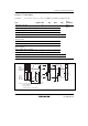
Table 28.9 I
2
C Bus Timing
Conditions: V
CC
= 3.0 V to 3.6 V, V
SS
= 0 V, φ = 8 MHz to maximum operating frequency
Item Symbol Min. Typ. Max. Unit
Test
Conditions
SCL input cycle time t
SCL
12 ⎯ ⎯
SCL input high pulse width t
SCLH
3 ⎯ ⎯
SCL input low pulse width t
SCLL
5 ⎯ ⎯
SCL, SDA input rise time t
Sr
⎯ ⎯ 7.5*
t
cyc
SCL, SDA input fall time t
Sf
⎯ ⎯ 300 ns
SCL, SDA input spike pulse
elimination time
t
SP
⎯ ⎯ 1
SDA input bus free time t
BUF
5 ⎯ ⎯
Start condition input hold time t
STAH
3 ⎯ ⎯
Retransmission start condition
input setup time
t
STAS
3 ⎯ ⎯
Stop condition input setup time t
STOS
3 ⎯ ⎯
Data input setup time t
SDAS
0.5 ⎯ ⎯
t
cyc
Data input hold time t
SDAH
0 ⎯ ⎯ ns
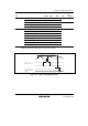
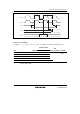
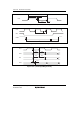
Figure
28.24
SCL, SDA capacitive load C
b
⎯ ⎯ 400 pF
Note: * 17.5 t
cyc
can be set according to the clock selected for use by the I
2
C module.
t
BUF
t
STAH
t
STAS
t
SP
t
STOS
t
SCLH
t
SCLL
t
Sf
t
Sr
t
SCL
t
SDAH
t
SDAS
P* S* Sr* P*
V
IH
V
IL
SDA0 to
SDA2
ExSDAA
ExSDAB
SCL0 to
SCL2
ExSCLA
ExSCLB
Note: * S, P, and Sr indicate the following conditions:
S: Start condition
P: Stop condition
Sr: Retransmission start condition
Figure 28.24 I
2
C Bus Interface Input/Output Timing