
Datasheet


Rev. 2.00 Sep. 28, 2009 Page xi of xl
REJ09B0452-0200
Item Page Revision (See Manual for Details)
15.1 Features
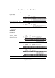
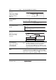
Figure 15.1 Block
Diagram of SCI
403 Figure amended
RxD
TxD
SCK
RSR
15.3 Register
Descriptions
Table 15.2 Register
Configuration
406 Table amended
Channel Register Name Abbreviation R/W
Initial
Value
Address
Data Bus
Width
Channel 1 Serial mode register_1 SMR_1 R/W H'00 H'FF88 8
Channel 2 Serial mode register_2 SMR_2 R/W H'00 H'FFA0 8
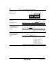
15.4.6 Serial Data
Reception
(Asynchronous Mode)
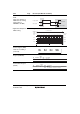
Figure 15.9 Sample
Serial Reception
Flowchart (1)
433 Figure amended
[5]
[6]
Clear RE bit in SCR to 0
Yes
All data received
End reception
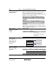
15.5.1 Multiprocessor
Serial Data Transmission
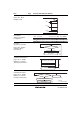
Figure 15.11 Sample
Multiprocessor Serial
Transmission Flowchart
437 Figure amended
[5]
Clear DR to 0 and set DDR to 1
Clear TE bit in SCR to 0
End transmission
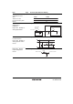
15.5.2 Multiprocessor
Serial Data Reception
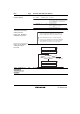
Figure 15.13 Sample
Multiprocessor Serial
Reception Flowchart (1)
439 Figure amended
Clear RE bit in SCR to 0
Error processing
(Continued on next page)
[5]
No
Yes
All data received
[6]
[Legend]
∨: Logical add (OR)
End reception