
Datasheet
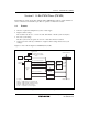


Section 9 14-Bit PWM Timer (PWMX)
Rev. 2.00 Sep. 28, 2009 Page 220 of 994
REJ09B0452-0200
9.2 Input/Output Pins
Table 9.1 lists the PWMX (D/A) module input and output pins.
Table 9.1 Pin Configuration
Pin Name Abbreviation I/O Function
PWMX output pin 0 PWX0 Output PWMX output of channel A
PWMX output pin 1 PWX1 Output PWMX output of channel B
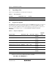
9.3 Register Descriptions
The PWMX (D/A) module has the following registers. The PWMX (D/A) registers are assigned to
the same addresses with other registers. The registers are selected by the IICE bit in the serial
timer control register (STCR). For details on the module stop control register, see section 26.1.3,
Module Stop Control Registers H, L, A, and B (MSTPCRH, MSTPCRL, MSTPCRA,
MSTPCRB).
Table 9.2 Register Configuration
Register Name Abbreviation R/W Initial Value Address
Data Bus
Width
PWMX (D/A) counter H DACNTH R/W H'00 H'FFA6
H'FEA6*
8
PWMX (D/A) counter L DACNTL R/W H'03 H'FFA7
H'FEA7*
8
PWMX (D/A) data register AH DADRAH R/W H'FF H'FFA0
H'FEA0*
8
PWMX (D/A) data register AL DADRAL R/W H'FF H'FFA1
H'FEA1*
8
PWMX (D/A) data register BH DADRBH R/W H'FF H'FFA6
H'FEA6*
8
PWMX (D/A) data register BL DADRBL R/W H'FF H'FFA7
H'FEA7*
8
PWMX (D/A) control register DACR R/W H'30 H'FFA0
H'FEA0*
8
Peripheral clock select register PCSR R/W H'00 H'FF82 8
Notes: The same addresses are shared by DADRA and DACR, and by DADRB and DACNT.
Switching is performed by the REGS bit in DACNT or DADRB.
* Upper address: when RELOCATE = 0
Lower address: when RELOCATE = 1