
Datasheet


Section 9 14-Bit PWM Timer (PWMX)
Rev. 2.00 Sep. 28, 2009 Page 234 of 994
REJ09B0452-0200
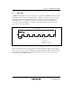
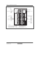
In this example, DADR = H'0207 (B'0000 0010 0000 0111). The output waveform is shown in
figure 9.7. Since CFS = 1 and the value of the upper eight bits is B'0000 0010, the high width of
the base pulse duty cycle is 2/256 × (T).
Since the value of the subsequent six bits is B'0000 01, an additional pulse is output only at the
location of base pulse No. 63 according to table 9.6. Thus, an additional pulse of 1/256 × (T) is to
be added to the base pulse.
1 conversion cycle
Base pulse
High width: 2/256 × (T)
Base pulse
2/256 × (T)
Additional pulse
1/256 × (T)
Base cycle Base cycle
Base cycle
No. 1No. 0 No. 63
Additional pulse output location
Figure 9.7 Output Waveform when DADR = H'0207 (OS = 1)
However, when CFS = 0 (base cycle = resolution (T) × 64), the duty cycle of the base pulse is
determined by the upper six bits and the locations of the additional pulses by the subsequent eight
bits with a method similar to as above.