
Datasheet


Section 15 Serial Communication Interface (SCI)
Rev. 2.00 Sep. 28, 2009 Page 409 of 994
REJ09B0452-0200
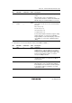
Bit Bit Name Initial Value R/W Description
2 MP 0 R/W Multiprocessor Mode (enabled only in asynchronous
mode)
When this bit is set to 1, the multiprocessor
communication function is enabled. The PE bit and
O/E bit settings are invalid in multiprocessor mode.
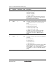
1
0
CKS1
CKS0
0
0
R/W
R/W
Clock Select 1 and 0
These bits select the clock source for the baud rate
generator.
00: φ clock (n = 0)
01: φ/4 clock (n = 1)
10: φ/16 clock (n = 2)
11: φ/64 clock (n = 3)
For the relation between the bit rate register setting
and the baud rate, see section 15.3.9, Bit Rate
Register (BRR). n is the decimal display of the value
of n in BRR (see section 15.3.9, Bit Rate Register
(BRR)).
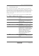
• Bit Functions in Smart Card Interface Mode (when SMIF in SCMR = 1)
Bit Bit Name Initial Value R/W Description
7 GM 0 R/W GSM Mode
Setting this bit to 1 allows GSM mode operation. In
GSM mode, the TEND set timing is put forward to
11.0 etu* from the start and the clock output control
function is appended. For details, see section
15.7.8, Clock Output Control.
6 BLK 0 R/W Setting this bit to 1 allows block transfer mode
operation. For details, see section 15.7.3, Block
Transfer Mode.
5 PE 0 R/W Parity Enable (valid only in asynchronous mode)
When this bit is set to 1, the parity bit is added to
transmit data before transmission, and the parity bit
is checked in reception. Set this bit to 1 in smart
card interface mode.