
Datasheet


Section 1 Overview
Rev. 2.00 Sep. 28, 2009 Page 19 of 994
REJ09B0452-0200
1.4.3 Pin Functions
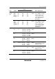
Table 1.4 Pin Functions
Pin No.
Type Symbol TFP-144V BP-176V TLP-145V I/O Name and Function
VCC 1, 36, 86 A1, J15,
P1, P2
B1, M1,
H10
Input Power supply pins. Connect all
these pins to the system power
supply. Connect the bypass
capacitor between VCC and VSS
(that is located near these pins).
VCL 13 F1 E1 Input External capacitance pin for
internal step-down power. Connect
this pin to VSS through an external
capacitor (that is located near this
pin) to stabilize internal step-down
power.
Power
supply
VSS 7, 42, 95,
111, 139
D1, D2,
P4, R4,
F12, F13,
B13,
A13, A4,
B4
D2, L3,
F10, B11,
C5
Input Ground pins. Connect all these
pins to the system power supply
(0 V).
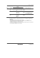
XTAL 143 A2 A3 Input
EXTAL 144 B2 A2 Input
For connection to a crystal
resonator. An external clock can be
supplied from the EXTAL pin. For
an example of crystal resonator
connection, see section 25, Clock
Pulse Generator.
φ 18 H1 F4 Output Supplies the system clock to
external devices.
EXCL 18 H1 F4 Input
Clock
ExEXCL 32 M3 K1 Input
32.768 kHz external sub clock
should be supplied. To which pin
the external clock is input can be
selected from the EXCL or
ExEXCL pin.
Operating
mode
control
MD2
MD1
25
9
K1
E2
H1
D1
Input These pins set the operating mode.
Inputs at these pins should not be
changed during operation.
System
control
RES 8 E3 D3 Input Reset pin. When this pin is low, the
chip is reset.