
Datasheet


Section 1 Overview
Rev. 2.00 Sep. 28, 2009 Page 24 of 994
REJ09B0452-0200
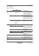
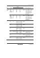
Pin No.
Type Symbol TFP-144V BP-176V TLP-145V I/O Name and Function
FSISS 113 D11 A11 Output FSI slave select pin
FSICK 114 A12 C11 Output Clock output pin
FSIDI 115 C11 B10 Input Receive data input pin
FSI
interface
(FSI)
FSIDO 116 B11 C10 Output Transmit data output pin
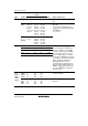
CIR
interface
(CIR)
CIRI 26 K2 J2 Input Receive data input pin
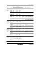
AN15 to
AN0
59 to 66,
75 to 68
M10, N10,
R10, P10,
N11, R11,
P11, M11,
P15, N13,
R15, P14,
R14, P13,
R13, N12
L7, K9, N8,
M9, L8,
K10, N9,
M10, L12,
N13, M13,
N12, N11,
L10, M11,
N10
Input Analog input pins
AVCC 76 N14, N15 M12 Input Analog power supply pin for
the A/D converter.
When the A/D converter is
not used, this pin should be
connected to the system
power supply (+3 V).
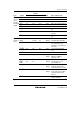
A/D
converter
AVref 77 M14, M15 L11 Input Reference power supply pin
for the A/D converter.
When the A/D converter is
not used, this pin should be
connected to the system
power supply (+3 V).
AVSS 67 R12, P12 L9 Input Ground pin for the A/D
converter. This pin should be
connected to the system
power supply (0 V).