
Datasheet

Section 21 FSI Interface
Rev. 2.00 Sep. 28, 2009 Page 703 of 994
REJ09B0452-0200
21.4 Operation
21.4.1 LPC/FW Memory Cycles
In LPC/FW memory read and write cycles, data is transferred using LAD3 to LAD0
synchronously with LCLK. The order of data transfer is shown in table 21.4. In a cycle returning
synchronization signal from the slave, the slave usually returns B'1010 to notify the host of error
occurrence; while the FSI in this LSI always returns B'0000 (Ready) or B'0110 (Long wait).
The FSI becomes busy if the received address matches an address in the host accessible range set
in the registers (FSIHBARH, FSIHBARL, FSISR, and CMDHBAR), and outputs a turn-around
signal to return to the idle state.
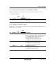
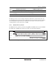
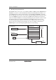
Table 21.4 LPC Memory Read/Write Cycles
LPC Memory Read Cycles LPC Memory Write Cycles
State
Counts Content Driven by Value (3 to 0) Content Driven by Value (3 to 0)
1 Start Host 0000 Start Host 0000
2 Cycle type/
direction
Host 0100 Cycle type/
direction
Host 0110
3 Address 1 Host bit 31 to bit 28 Address 1 Host bit 31 to bit 28
4 Address 2 Host bit 27 to bit 24 Address 2 Host bit 27 to bit 24
5 Address 3 Host bit 23 to bit 20 Address 3 Host bit 23 to bit 20
6 Address 4 Host bit 19 to bit 16 Address 4 Host bit 19 to bit 16
7 Address 5 Host bit 15 to bit 12 Address 5 Host bit 15 to bit 12
8 Address 6 Host bit 11 to bit 8 Address 6 Host bit 11 to bit 8
9 Address 7 Host bit 7 to bit 4 Address 7 Host bit 7 to bit 4
10 Address 8 Host bit 3 to bit 0 Address 8 Host bit 3 to bit 0
11 Turn-around
(recovery)
Host 1111 Data 1 Host bit 3 to bit 0
12 Turn-around None ZZZZ Data 2 Host bit 7 to bit 4
13 Wait* Slave 0110 Turn-around
(recovery)
Host 1111