
Datasheet
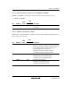


Section 21 FSI Interface
Rev. 2.00 Sep. 28, 2009 Page 705 of 994
REJ09B0452-0200
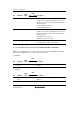
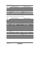
FW Memory Read Cycles FW Memory Write Cycles
State
Counts
Content Driven by Value (3 to 0) Content Driven by Value (3 to 0)
17 Turn-around
(recovery)
Slave 1111 Turn-around
(recovery)
Slave 1111
18 Turn-around None ZZZZ Turn-around None ZZZZ
Note: * The number of wait cycles depends on the system clock.
The FSI supports byte, word, and longword transfers of FW memory read and write cycles. In
word transfer, the least address bit is fixed to B'0; while in longword transfer, the lower 2 bits are
fixed to B'00. When longword transfers of FW memory write cycles are used, the maximum
operating frequency of the system clock is 10 MHz.
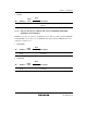
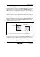
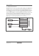
21.4.2 SPI Flash Memory Transfer
The SPI flash memory transfer is performed using FSIDO and FSIDI synchronously with FSICK.
The initial value of FSICK can be either fixed to high or low through programming.
FSISS
FSICK
FSIDO
FSIDI
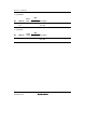
Bit7
Bit7
Bit6
Bit6
Bit5
Bit5
Bit4
Bit4
Bit3
Bit3
Bit2
Bit2
Bit1
Bit1
Bit0
Bit0
MSB LSB
MSB
LSB
Figure 21.2 Example of SPI Flash Memory Transfer