
Datasheet


Section 21 FSI Interface
Rev. 2.00 Sep. 28, 2009 Page 708 of 994
REJ09B0452-0200
(2) Byte/Page-Program Instruction
If an LPC/FW memory write cycle occurs while the AAIE bit in FSICR1 and the FSIDMYE bit in
FSILSTR1 are cleared to 0, and the FLDCT bit in SLCR and the FLWAIT bit in SLCR are set to
1, the SPI flash memory address and write data are stored in FSIAR and FSIWDR, respectively.
Then, the SPI flash memory address, the write data, and the Byte/Page-Program instruction which
is stored in FSIPPINS in advance are transferred to FSITDR. After SYNC (long wait) has been
returned, the TE bit in FSICR2 is set, starting the Byte/Page-Program instruction execution. When
the transmission has been completed, SYNC (Ready) and TAR are returned to the host. To
execute the Byte-Program instruction, byte transfer access in LPC memory write cycle or FW
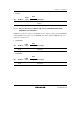
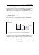
memory write cycle should be performed. Figure 21.4 shows an example of data transfer to
FSITDR. Figure 21.5 shows the Page-Program instruction execution timing.
FSIWDR[31:0]
FSIAR[23:0]
FSIPPINS[7:0]
H'67_45_23_01
H'06_4A_70
H'02
FSISFR
FSIWDR[31:24]
FSITDR7
FSITDR6
FSITDR0
FSIDO
FSIWDR[23:16]
FSIWDR[15:8]
FSIWDR[7:0]
FSIAR[7:0]
FSIAR[15:8]
FSIAR[23:16]
H'67
H'45
H'23
H'01
H'70
H'4A
H'06
H'02
Figure 21.4 Data Transfer to FSITDR (Example)