
Datasheet


Section 21 FSI Interface
Rev. 2.00 Sep. 28, 2009 Page 715 of 994
REJ09B0452-0200
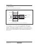
(2) FSI Command Write
If an LPC/FW memory write cycle for the FSI command space occurs, the FSI performs the FSI-
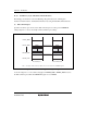
FLASH command write operation. Figure 21.12 shows an example of FSI Command write
operation.
CMDHBAR: H'EFFF
H'EFFF_0000
*
H'EFFF_F000
H'EFFF_F00F
H'EFFF_FFFF
Host address
CMD0
CMD1
CMDE
CMDF
FSICMDR[7:0]
FSICMDI
FSICMDIE
CMDBUSY
Command data (H'00 to H'FF)
B'0 B'1
B'0 B'1
B'1
Interrupt requests
→
→
Note:
*
The upper 16 bits of the host address are set to the value in the CMDHBAR register.
Figure 21.12 FSI Command Write Operation (Example)
As shown in figure 21.12, if a host address ranging from H'EFFF_F000 to H'EFFF_F00F is
accessed in LPC/FW memory write cycle while the CMDHBAR register is set to H'EFFF, the
write data is stored in FSICMDR, and then the CMDBUSY and FSICMDI flags in FSILSTR1 are
set to 1. In this case, an interrupt is requested according to the FSICMDIE state. Sync is not
returned if the host address to be input is out of the determined range. In FSI command write, no
wait cycle will be inserted to the LPC bus cycle. If the CMDBUSY flag is set to 1, Sync is not
returned during the operations other than FSI command read.