
Datasheet


Section 21 FSI Interface
Rev. 2.00 Sep. 28, 2009 Page 717 of 994
REJ09B0452-0200
(4) FSI Dummy Write
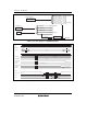
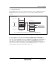
Figure 21.14 shows an example of FSI dummy write.
FSI Dummy Write
FSIHBAR: H'231F
FSISR: H'00 (1 MB)
CMDHBAR: H'EFFF
H'73
Host address
Host address
H'2325_4A76
FSIDMYE
FSIWDR[31:0]
FSIAR[23:0]
B'1
H'0000_0073
H'06_4A76
FSIDMYE
FSIWDR[31:0]
FSIAR[23:0]
B'0
H'0000_00D4
H'0F_1BC3
Byte-Program
H'232E_1BC3
H'D4 H'D4
SPI Flash memory
H'0F_1BC3
Flash memory address
Figure 21.14 FSI Dummy Write (Example)
As shown in figure 21.14, if an LPC/FW memory write cycle occurs while the FSIDMYE bit in
FSILSTR1 is 1, the FSI does not access the SPI flash memory but stores the SPI flash memory
address and write data in FSIAR and FSIWDR, respectively.