
Datasheet

Section 24 Flash Memory
Rev. 2.00 Sep. 28, 2009 Page 756 of 994
REJ09B0452-0200
(5) When Programming/Erasing is Executed Consecutively
When processing does not end by 128-byte programming or 1-block erasure, consecutive
programming/erasing can be realized by updating the start address of the programming destination
and program data, or the erase block number. Since the downloaded on-chip program is left in the
on-chip RAM even after programming/erasing completes, download and initialization are not
required when the same processing is executed consecutively.
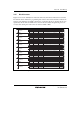
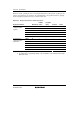
24.6 Input/Output Pins
The flash memory is controlled through the input/output pins shown in table 24.2.
Table 24.2 Pin Configuration
Abbreviation I/O Function
RES Input Reset
MD2, MD1 Input Set operating mode of this LSI
TxD1 Output Serial transmit data output (used in boot mode)
RxD1 Input Serial receive data input (used in boot mode)