
Datasheet

Section 24 Flash Memory
Rev. 2.00 Sep. 28, 2009 Page 759 of 994
REJ09B0452-0200
24.7.1 Programming/Erasing Interface Registers
The programming/erasing interface registers are 8-bit registers that can be accessed only in bytes.
These registers are initialized by a power-on reset.
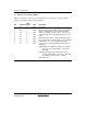
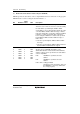
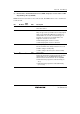
(1) Flash Code Control/Status Register (FCCS)
FCCS monitors errors during programming/erasing the flash memory and requests the on-chip
program to be downloaded to the on-chip RAM.
Bit Bit Name
Initial
Value
R/W Description
7
6
5
⎯
⎯
⎯
1
0
0
R
R
R
Reserved
These are read-only bits and cannot be modified.
4 FLER 0 R Flash Memory Error
Indicates that an error has occurred during programming
or erasing the flash memory. When this bit is set to 1,
the flash memory enters the error protection state.
When this bit is set to 1, high voltage is applied to the
internal flash memory. To reduce the damage to the
flash memory, the reset must be released after the reset
input period (period of RES = 0) of at least 100 μs.
0: Flash memory operates normally (Error protection is
invalid)
[Clearing condition]
• At a power-on reset
1: An error occurs during programming/erasing flash
memory (Error protection is valid)
[Setting conditions]
• When an interrupt, such as NMI, occurs during
programming/erasing.
• When the flash memory is read during
programming/erasing (including a vector read and
an instruction fetch).
• When the SLEEP instruction is executed during
programming/erasing (including software standby
mode).