
Datasheet


Section 27 List of Registers
Rev. 2.00 Sep. 28, 2009 Page 856 of 994
REJ09B0452-0200
27.1 Register Addresses (Address Order)
The data bus width indicates the numbers of bits.
The number of access states indicates the number of states based on the specified reference clock.
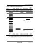
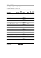
Register Name Abbreviation
Number
of bits Address Module
Data
Width
Access
States
Port 1 data direction register P1DDR 8 H'F900
(PORTS = 1)
PORT 8 2
Port 2 data direction register P2DDR 8 H'F901
(PORTS = 1)
PORT 8 2
Port 1 data register P1DR 8 H'F902
(PORTS = 1)
PORT 8 2
Port 2 data register P2DR 8 H'F903
(PORTS = 1)
PORT 8 2
Port 1 input data register P1PIN 8 H'F904 (Read)
(PORTS = 1)
PORT 8 2
Port 2 input data register P2PIN 8 H'F905 (Read)
(PORTS = 1)
PORT 8 2
Port 1 pull-up MOS control register P1PCR 8 H'F906
(PORTS = 1)
PORT 8 2
Port 2 pull-up MOS control register P2PCR 8 H'F907
(PORTS = 1)
PORT 8 2
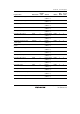
Port 3 data direction register P3DDR 8 H'F910
(PORTS = 1)
PORT 8 2
Port 4 data direction register P4DDR 8 H'F911
(PORTS = 1)
PORT 8 2
Port 3 data register P3DR 8 H'F912
(PORTS = 1)
PORT 8 2
Port 4 data register P4DR 8 H'F913
(PORTS = 1)
PORT 8 2
Port 3 input data register P3PIN 8 H'F914 (Read)
(PORTS = 1)
PORT 8 2
Port 4 input data register P4PIN 8 H'F915 (Read)
(PORTS = 1)
PORT 8 2
Port 3 pull-up MOS control register P3PCR 8 H'F916
(PORTS = 1)
PORT 8 2