
Datasheet


Section 7 I/O Ports
Rev. 3.00 Sep. 28, 2009 Page 135 of 910
REJ09B0350-0300
Section 7 I/O Ports
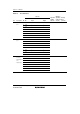
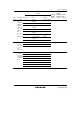
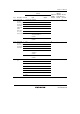
Table 7.1 lists the port functions. The pins of each port also have other functions such as
input/output pins of on-chip peripheral modules or interrupt input pins. Each I/O port includes a
data direction register (DDR) that controls input/output, a data register (DR) that stores output
data, and a port input data register (PIN) used to read the pin states. Port E does not have a DR or
a DDR register.
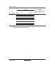
Ports 1 to 3, 6, 9, B to D, F, H, and J have internal input pull-up MOSs and a pull-up MOS control
register (PCR) that controls the on/off state of the input pull-up MOSs.
In addition, ports 1 to 3, C, and D can drive a LED (5 mA sink current). P52, P97, P86, P42, ports
A, G, and I are NMOS push-pull outputs and 5-V tolerant inputs. PE4 and PE2 to PE0 are 5-V
tolerant inputs.
Ports I and J are not supported by TFP-144V and TLP-145V.