
Datasheet


Section 7 I/O Ports
Rev. 3.00 Sep. 28, 2009 Page 149 of 910
REJ09B0350-0300
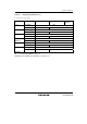
7.1.5 Output Data Register (PnODR) (n = A to D and F to J)
ODR is a register that stores output data for ports. The upper two bits in PHODR are reserved.
Bit Bit Name Initial Value R/W Description
7 Pn7ODR 0 R/W
6 Pn6ODR 0 R/W
5 Pn5ODR 0 R/W
4 Pn4ODR 0 R/W
3 Pn3ODR 0 R/W
2 Pn2ODR 0 R/W
1 Pn1ODR 0 R/W
ODR stores the output data for the pins that are
used as the general output port.
0 Pn0ODR 0 R/W
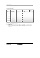
7.1.6 Noise Canceller Enable Register (PnNCE) (n = 6, C, and G)
NCE enables or disables the noise cancel circuit at port n pins in bit units.
Bit Bit Name Initial Value R/W Description
7 Pn7NCE 0 R/W
6 Pn6NCE 0 R/W
5 Pn5NCE 0 R/W
4 Pn4NCE 0 R/W
3 Pn3NCE 0 R/W
2 Pn2NCE 0 R/W
1 Pn1NCE 0 R/W
Noise cancel circuit is enabled when a bit in this
register is set to 1, and the pin setting state is
fetched in P6DR or PnPIN in the sampling cycle
set by the PnNCCS.
0 Pn0NCE 0 R/W